Mastering FIB-SEM Sample Preparation: A Complete Guide for Cross-Sectional Analysis in Biomedical Research
This comprehensive guide details the principles, methodology, optimization, and validation of FIB-SEM sample preparation for high-resolution cross-sectional analysis.
Mastering FIB-SEM Sample Preparation: A Complete Guide for Cross-Sectional Analysis in Biomedical Research
Abstract
This comprehensive guide details the principles, methodology, optimization, and validation of FIB-SEM sample preparation for high-resolution cross-sectional analysis. Tailored for researchers, scientists, and drug development professionals, it covers foundational concepts, step-by-step protocols, advanced troubleshooting techniques, and comparative validation strategies. The article empowers users to generate artifact-free, high-fidelity samples, crucial for elucidating ultrastructural details in cells, tissues, and materials, thereby advancing discoveries in biomedicine, pharmacology, and clinical diagnostics.
What is FIB-SEM and Why is it Critical for Cross-Sectional Analysis in Biomedical Research?
Application Notes: Principles and Quantitative Capabilities
Focused Ion Beam-Scanning Electron Microscopy (FIB-SEM) is an integrated correlative microscopy technique that enables site-specific milling, ablation, and deposition of materials with nanometer precision (via the ion beam) and subsequent high-resolution imaging (via the electron beam). It is a cornerstone tool for cross-sectional analysis, 3D tomography, and failure analysis in materials science, semiconductor industries, and life sciences, including drug development.
Core Quantitative Specifications (Typical Current Systems): The table below summarizes key performance metrics of modern FIB-SEM instruments based on a live search of specifications from leading manufacturers (e.g., Thermo Fisher Scientific, ZEISS, TESCAN, Hitachi High-Tech).
| Parameter | Gallium (Ga+) FIB-SEM | Plasma FIB-SEM (Xe+, Ar+) | Multibeam (Electron + Ion + Light) | Primary Application in Sample Prep |
|---|---|---|---|---|
| Ion Beam Resolution | 2.5 - 7 nm @ 30 kV | 10 - 20 nm @ 30 kV | 2.5 - 5 nm (Ga+); ~1 µm (Light) | Precise site-specific milling |
| SEM Resolution | 0.6 - 1.2 nm @ 15 kV (in-lens) | 0.8 - 1.5 nm @ 15 kV | 0.6 - 1.0 nm @ 15 kV | High-resolution imaging of milled surface |
| Milling Rate (Si) | ~1 µm³/nC (30 kV, 10 nA) | ~10-50X faster than Ga+ (30 kV, 1.5 µA) | Similar to respective ion source | Speed for large cross-sections or volumes |
| Cross-section Polish Quality | < 5 nm roughness (with final low-kV polish) | < 10-20 nm roughness | < 5 nm roughness | Suitability for high-resolution imaging post-mill |
| Typical Lamella Thickness | 50 - 150 nm for TEM | 80 - 200 nm for TEM | 50 - 150 nm | Creating electron-transparent membranes |
| 3D Tomography Voxel Size | 5 x 5 x 5 nm³ (serial slicing) | 15 x 15 x 15 nm³ (large volumes) | 5 x 5 x 5 nm³ (with correlative data) | Resolution in reconstructed 3D volumes |
Key Applications in Research & Drug Development:
- Pharmaceutical Granule/Tablet Analysis: Cross-sectional mapping of active pharmaceutical ingredient (API) distribution, excipient morphology, and coating layer integrity.
- Battery & Fuel Cell Research: 3D nano-tomography of electrode degradation, solid-electrolyte interphase (SEI) layer formation, and pore structure analysis.
- Biological Tissue & Cell Ultrastructure: Serial block-face imaging for 3D reconstruction of organelles, neuronal circuits, or pathogen-host interfaces (after appropriate staining and embedding).
- Nanoparticle & Drug Delivery System Characterization: Precise cross-sectioning of liposomes, polymeric nanoparticles, or antibody-drug conjugates to analyze core-shell structure and composition.
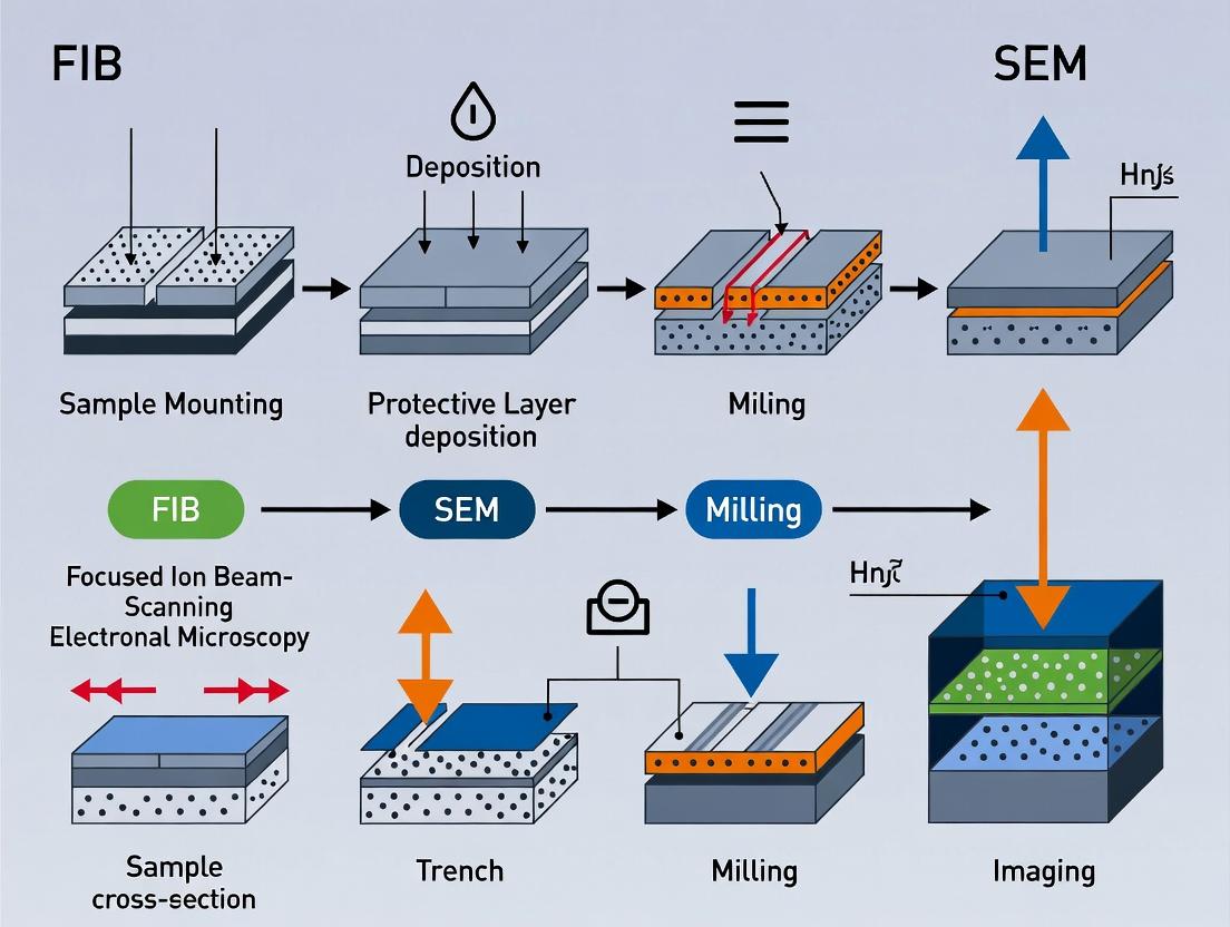
Title: FIB-SEM Cross-Section & 3D Tomography Workflow
Experimental Protocols
Protocol 1: Standard Site-Specific Cross-Section Preparation for Coated Pharmaceutical Tablet
Objective: To expose a pristine sub-surface interface (e.g., coating-core) for high-resolution SEM analysis of layer uniformity and adhesion.
Materials: See "The Scientist's Toolkit" below.
Methodology:
- Mounting: Adhere the tablet to an aluminum stub using conductive carbon tape. Ensure the region of interest (ROI) is accessible and the stub is securely placed in the FIB-SEM stage.
- Conductive Coating: Sputter-coat the sample with a 10-20 nm layer of Au/Pd to prevent charging during ion and electron beam procedures.
- Load & Pump Down: Transfer the sample to the FIB-SEM chamber and achieve high vacuum (<5 x 10⁻⁵ mBar).
- Navigation: Use the electron beam (2-5 kV, 0.1 nA) to locate the precise ROI for cross-sectioning.
- Protective Deposition:
- Switch to the ion beam view. Use the gas injection system (GIS) to deposit a 1 µm thick platinum (Pt) strap directly over the ROI line. Typical conditions: 30 kV Ga+ ion beam, 0.3 nA, ~5 minutes.
- Rough Trench Milling:
- Define a rectangular milling pattern on either side of the Pt strap. Use a high beam current (e.g., 7-15 nA at 30 kV) to mill two trenches, leaving a thin wall containing the ROI protected by the Pt cap.
- Mill to a depth of 15-20 µm.
- Fine Polish & Undercutting:
- Progressively reduce the ion beam current (3 nA, 1 nA, 0.5 nA) to polish the cross-sectional face, removing ion beam damage.
- Tilt the stage to ~45-52° to present the polished face to the electron beam.
- Use a very low current (0.1 nA or less) for a final "clean-up" polish to achieve an imaging-ready surface.
- Imaging:
- With the stage tilted, use the electron beam at low voltage (2-5 kV) and a through-the-lens (TLD) detector to acquire high-resolution secondary electron (SE) and backscattered electron (BSE) images of the cross-section.
Protocol 2: Serial Block-Face Imaging for 3D Reconstruction of a Biological Specimen (Embedded Tissue)
Objective: To automatically generate a stack of images for 3D ultrastructural analysis.
Materials: Resin-embedded, heavy-metal stained (e.g., OsO₄, uranyl acetate) tissue block, trimmer, conductive silver paint.
Methodology:
- Sample Preparation: Trim the resin block to expose the tissue surface. Mount on a SEM stub using conductive paint. Apply a conductive metal coating (Au/Pd or carbon).
- Initial Face Preparation: Inside the FIB-SEM, use the ion beam at a moderate current (1-3 nA) to mill a large, flat, clean surface over the entire ROI.
- Automated Serial Slice-and-View Setup:
- Define a milling pattern covering the ROI area. Set the slice thickness (e.g., 10 nm).
- Define the imaging frame and parameters (e.g., 3 kV, 0.1 nA, 4096 x 3536 pixels, dwell time 1-3 µs).
- Run Automation Sequence:
- The system executes a repeated cycle: a. Mill away one slice thickness using the ion beam (e.g., 30 kV, 0.3 nA). b. Stop ion beam. c. Image the newly exposed surface with the SEM. d. Store the image. e. Realign if necessary (using automated feature tracking).
- Post-processing: Align the image stack using software (e.g., Fiji/TrakEM2, Amira, Avizo). Segment structures of interest and perform 3D volume rendering and quantitative analysis.
The Scientist's Toolkit: Key Research Reagent Solutions for FIB-SEM
| Item | Function | Typical Example/Formula |
|---|---|---|
| Conductive Adhesive Tape/Carbon Paste | Provides electrical and mechanical grounding of the sample to the stub, preventing charging. | Carbon double-sided tape; Silver Dag colloidal silver paint |
| Sputter Coater (Au/Pd Target) | Applies a thin, continuous conductive metal layer on non-conductive samples to dissipate charge. | 80/20 Gold/Palladium target; 10-20 nm coating thickness |
| Gas Injection System (GIS) Precursors | Allows ion/electron beam induced deposition of protective or conductive materials, or enhanced etching. | (CH₃)₃Pt(CpCH₃) for Pt deposition; XeF₂ for enhanced etching of organics/copper; WF₆ for Tungsten deposition |
| Heavy Metal Stains (Life Sciences) | Infiltrate biological samples with high-atomic number elements to provide SEM contrast and stabilize structure. | Osmium tetroxide (OsO₄), Uranyl acetate, Lead citrate |
| Conductive Embedding Resins | Embed and support delicate samples (e.g., tissue, powders) while providing electrical conductivity. | EPON resin mixed with silver powder; Low-viscosity epoxy with carbon nanotubes |
| Micromanipulator Needles/Probes | For in-situ lift-out of TEM lamellae or manipulation of milled fragments. | OmniProbe style needles with tungsten or platinum tips |
| Calibration Reference Samples | For daily performance checks of both SEM resolution and FIB milling alignment/accuracy. | Gold-on-carbon particle standard; Silicon grating with pre-defined trenches |
Within the broader thesis on FIB-SEM for cross-sectional analysis, the core principle is that the analysis plane is perpendicular to the sample surface or a specific feature of interest. This demands unique preparation protocols because the region of interest (ROI) is often buried, and the preparation must preserve the structural and chemical integrity of that specific 2D plane through a 3D volume. Inadequate preparation leads to artifacts, misinterpretation, and non-reproducible data, particularly critical for research in drug development, where understanding cellular ultrastructure or material interfaces is paramount.
Application Notes: Challenges & Quantitative Comparisons
Table 1: Comparative Analysis of Sample Prep Artefacts in Cross-Sectional FIB-SEM
| Artefact Type | Cause in Conventional Prep | Impact on Cross-Sectional Analysis | Mitigation via Dedicated Cross-Sectional Prep |
|---|---|---|---|
| Curtaining | Uneven milling due to heterogeneous material hardness. | Obscures true interface geometry, masks compositional layers. | Use of a protective surface coating (Pt, C), low-angle polishing mills. |
| Redeposition | Milled material re-adheres to the cut surface. | Creates false topological features, blocks underlying structure. | Sequential cleaning cross-sections, gas-assisted etching (XeF2, I2). |
| Ion Beam Damage | High-energy Ga+ ion implantation and amorphization. | Alters crystal structure, creates pseudo-porosity (in biologicals). | Use of low-kV final polishing steps (<5 kV), cryogenic preparation. |
| Stress Relief | Mechanical sectioning (e.g., cleaving) releases internal stress. | Induces cracks and delamination at interfaces, void formation. | In-situ lift-out and FIB polishing to minimize macro-scale stress. |
| Shrinkage/Swelling | Poor chemical fixation or dehydration (biologicals). | Distorts cellular dimensions, collapses luminal structures. | Optimized cryo-fixation (HPF) and resin embedding protocols. |
Table 2: Protocol Efficacy Metrics (Summarized from Recent Literature)
| Preparation Protocol | Target Material | Reported Surface Roughness (Ra) | Preserved Layer Integrity (Y/N) | Total Prep Time (hrs) |
|---|---|---|---|---|
| Standard Cleaving & Sputter Coat | Semiconductor multilayer | >50 nm | N (severe delamination) | 1.5 |
| Conventional FIB Milling (30kV) | Battery electrode composite | 10-15 nm | Partial (ion damage layer ~30nm) | 3.0 |
| Cryo-FIB on HPF Biological | Mammalian tissue | <5 nm* | Y (membranes intact) | 8.0+ |
| XeF2-Assisted FIB Milling | PCB with polymer/copper | ~3 nm | Y (clean interface) | 4.5 |
| Low-kV Final Polish (2kV) | Ceramic coating on alloy | <1 nm | Y (atomic layers visible) | 5.0 |
*Estimated from published micrographs.
Experimental Protocols
Protocol A: Cryogenic FIB-SEM Cross-Section for Soft Biological Materials
Objective: To prepare an artifact-free cross-section of high-pressure frozen (HPF), freeze-substituted cultured cells for in-lens analysis of organelle morphology.
- HPF & Freeze Substitution: Culture cells on a suitable carrier. High-pressure freeze using a system like Leica EMPACT2. Transfer to automated freeze-substitution system (e.g., Leica AFS2) in anhydrous acetone with 2% OsO4 and 0.1% uranyl acetate at -90°C for 72 hrs, warming to 4°C.
- Resin Embedding: Infiltrate with graded series of EPON resin in acetone (30%, 50%, 70%, 100%) over 24 hrs. Polymerize in fresh resin at 60°C for 48 hrs.
- Block Trimming & Coating: Roughly trim the block face with a razor. Mount on a SEM stub. Sputter coat with a 10 nm conductive Ir layer.
- FIB-SEM Preparation: Mount in a dual-beam FIB-SEM with a cryo-stage pre-cooled to below -140°C. Use the GIS to deposit a 1 µm organometallic Pt protective strap over the ROI at 10 kV. Perform coarse trench milling at 30 kV, 3 nA. Perform fine polishing sequentially at 5 kV, 50 pA and finally at 2 kV, 15 pA.
- Imaging: Image the cross-section at 2-5 kV using the in-lens SE detector.
Protocol B: XeF2-Assisted FIB Cross-Section for Polymer-Metal Composites
Objective: To prepare a cross-section through a printed circuit board (PCB) via to examine copper-polymer adhesion without redeposition.
- Sample Mounting: Cleave a small section of the PCB containing the ROI. Mount on a standard SEM stub with conductive carbon tape. Apply a conductive silver paint border to enhance grounding.
- Protective Coating: Use the electron beam to deposit a 500 nm carbon layer locally over the via. Use the ion beam GIS to deposit a 1 µm platinum cap over the carbon layer.
- Initial Trench Milling: Mill two large trenches on either side of the via using the FIB at 30 kV, 7 nA to create a free-standing lamella of the via.
- Gas-Assisted Etching (GAE): Introduce XeF2 gas via the GIS needle, positioned ~100 µm from the surface. Use a patterned ion beam scan at 30 kV, 0.5 nA. The XeF2 reacts preferentially with the polymer/glass fiber, etching it and volatilizing the products, while leaving the copper largely unaffected.
- Final Cleaning: Perform a final, brief, low-current (50 pA) FIB polish at 5 kV without gas to remove any minor redeposits.
- Analysis: Image at 5 kV and perform EDS mapping to analyze the interface chemistry.
Visualization: Workflows & Pathways
Title: Standard FIB-SEM Cross-Section Workflow
Title: Cryo-FIB-SEM Prep for Biologicals
The Scientist's Toolkit: Research Reagent Solutions
Table 3: Essential Materials for Cross-Sectional FIB-SEM Preparation
| Item | Function in Cross-Sectional Prep | Example/Note |
|---|---|---|
| Organometallic Gas Injection System (GIS) Precursors | In-situ deposition of conductive, protective layers (Pt, W, C) precisely over the ROI to prevent curtaining and charge buildup. | (CH₃)₃CH₃C₅H₄Pt (Pt precursor) or W(CO)₆. |
| XeF₂ or I₂ Gas Etchants | For gas-assisted etching (GAE). Selectively enhances etch rate of specific materials (polymers, oxides, organics), reducing redeposition and ion damage. | Critical for composites and devices with heterogeneous materials. |
| Conductive Mounting Adhesives | Provides stable, electrical, and mechanical grounding of the sample to the stub, eliminating charging artifacts during milling/imaging. | Silver dag, carbon cement, or conductive copper tape. |
| High-Pressure Freezing (HPF) Media | For biologicals: Physically immobilizes cellular water as vitreous (non-crystalline) ice, preserving ultrastructure in a near-native state for cryo-FIB. | 20% Dextran, 1-Hexadecene, or proprietary media like "Laromidium". |
| Freeze Substitution Cocktails | For biologicals: Gradual replacement of ice with organic solvent and fixatives/stains at low temperature, preparing resin-embedded samples. | Acetone/Osmium Tetroxide/Uranyl Acetate or Tannic Acid mixtures. |
| Low-Shrinkage, Infiltrating Resins | Provides mechanical support for brittle or soft samples, enabling thin sectioning and stable milling. | EPON, Spurr's, or Lowicryl resins for EM. |
| FIB Lift-Out Micromanipulators | Needles or probes for extracting a prepared lamella and transferring it to a TEM grid for subsequent analysis (TEM, Atom Probe). | Omniprobe or Kleindiek nanomanipulator systems. |
Application Notes
The integration of Focused Ion Beam-Scanning Electron Microscopy (FIB-SEM) in biomedical research has revolutionized our ability to visualize and analyze biological systems across scales. Within the context of a thesis on advanced FIB-SEM sample preparation for cross-sectional analysis, these applications are critical. The technique provides unparalleled 3D ultrastructural data, bridging the gap between cellular organelle function and the engineered complexity of nanoscale drug delivery systems (DDS). The following notes detail key applications supported by current research.
1. Organelle-Specific Pathology and Drug Targeting: FIB-SEM tomography enables the quantitative 3D analysis of organelle alterations in disease states, such as mitochondrial fragmentation in neurodegeneration or endoplasmic reticulum stress in cancer. This structural data is directly informing the rational design of organelle-targeted DDS. For instance, precise measurement of lysosomal volume and membrane integrity in treated versus untreated cells provides critical efficacy and toxicity readouts for nanotherapeutics.
2. Nanocarrier-Cell Interactions: The fate of polymeric nanoparticles, liposomes, and lipid nanoparticles (LNPs) upon cellular entry is a central question. FIB-SEM cross-sectioning, superior to TEM for visualizing large volumes, allows researchers to definitively locate carriers within cells—whether they are free in the cytosol, encapsulated in endosomes, or associated with specific organelles. This directly validates or refutes hypotheses regarding escape mechanisms and intracellular trafficking pathways.
3. Vaccine Delivery Systems: For mRNA vaccines utilizing LNPs, FIB-SEM is instrumental in characterizing both the morphology of the carrier itself and its interaction with immune cells. High-resolution cross-sectional imaging can reveal the disposition of mRNA cargo within the LNP core and the integrity of the bilayer after freeze-thaw cycles, linking structural properties to biological potency and stability.
4. Biomaterial and Tissue Engineering: Beyond cellular analysis, FIB-SEM is used to characterize the microstructure of porous scaffolds for tissue engineering and the interface between implanted biomaterials and host tissue at the nanoscale. This provides essential feedback for designing materials that direct cellular ingrowth and response.
Table 1: Quantitative FIB-SEM Analysis in Recent Biomedical Studies
| Application Focus | Key Measured Parameters | Typical Quantitative Findings (Range) | Primary Sample Preparation Challenge |
|---|---|---|---|
| Mitochondrial Dysfunction (e.g., Parkinson's) | Volume, Surface Area, Cristae Density | Volume: 0.1 - 0.5 µm³; Cristae Density: 15 - 40 µm²/µm³ | Preserving delicate cristae structure during dehydration. |
| Liposome Endosomal Escape | Distance of carrier from endosomal membrane, % of escaped carriers | Successful escape correlated with carriers <50 nm from membrane. Escape efficiency: 10-40% depending on formulation. | Distinguishing carrier material from cellular contents in BSE contrast. |
| mRNA-LNP Biodistribution (in vitro) | LNP core diameter, Bilayer thickness, Internalization count per cell | Core Dia: 40-80 nm; Bilayer: 4-6 nm; Uptake: 50-200 particles/cell in hepatocytes. | Preventing LNP dissolution or deformation during processing. |
| Scaffold-Cell Integration | Pore size, Cell infiltration depth, Focal adhesion density | Optimal pore size for osteogenesis: 200-400 µm; Cell infiltration: 100-500 µm after 7 days. | Charge dissipation in large, insulating polymer scaffolds. |
Experimental Protocols
Protocol 1: FIB-SEM Sample Preparation for Analyzing Nanoparticle Uptake in Cultured Cells
This protocol details the process for preparing adherent cell cultures to visualize internalized drug delivery nanoparticles.
Objective: To preserve the ultrastructure of cells and the integrity of internalized nanoparticles for cross-sectional milling and imaging via FIB-SEM.
Materials:
- Cultured cells (e.g., HeLa, HepG2) on a conductive silicon wafer or Thermanox coverslip.
- Primary fixative: 2.5% Glutaraldehyde in 0.1M Sodium Cacodylate buffer, pH 7.4.
- Secondary fixative: 1% Osmium Tetroxide in 0.1M Sodium Cacodylate buffer.
- En bloc contrast: 1% aqueous Uranyl Acetate.
- Ethanol series (30%, 50%, 70%, 90%, 100%, 100% anhydrous).
- Intermediate solvent: Anhydrous Acetone or Ethanol.
- Epoxy resin (e.g., Epon, Durcupan).
- Critical Point Dryer (optional, for alternative method).
- Sputter Coater.
Methodology:
- Fixation: Immediately after treatment with nanoparticles, remove culture medium and gently add primary fixative. Fix for 1-2 hours at room temperature or overnight at 4°C.
- Rinsing: Rinse cells 3x with 0.1M Sodium Cacodylate buffer (5 minutes each).
- Post-fixation: Incubate with 1% Osmium Tetroxide solution for 1 hour at 4°C in the dark.
- Rinsing: Rinse thoroughly with distilled water (3 x 5 minutes).
- En Bloc Staining: Incubate with 1% aqueous Uranyl Acetate overnight at 4°C in the dark.
- Dehydration: Dehydrate cells using a graded ethanol series (30%, 50%, 70%, 90%, 100%, 100% anhydrous), 10 minutes per step.
- Infiltrate & Embed:
- Prepare a 1:1 mixture of anhydrous solvent (acetone/ethanol) and epoxy resin. Apply to sample for 1-2 hours.
- Replace with 100% epoxy resin and infiltrate overnight on a rotator.
- Place fresh resin on the sample and polymerize at 60°C for 48 hours.
- Mounting & Conductive Coating:
- Mount the polymerized block on a standard SEM stub using conductive silver epoxy or carbon tape.
- Sputter coat the entire sample with a 10-20 nm layer of gold/palladium or apply a conductive carbon paint to the sides to ensure charge dissipation during FIB milling.
Protocol 2: FIB-SEM Tomography for 3D Mitochondrial Morphometry
This protocol describes the serial milling and imaging steps to generate a 3D reconstruction of mitochondria.
Objective: To acquire a stack of serial SEM images for the 3D volumetric analysis of organelles.
Materials:
- FIB-SEM system (e.g., TESCAN GAIA3, Zeiss Crossbeam).
- Sample prepared per Protocol 1, mounted in the FIB-SEM.
- Imaging software with alignment and segmentation capabilities (e.g., Fiji/ImageJ, Amira, Avizo).
Methodology:
- Sample Orientation: Using the SEM, locate the region of interest (ROI). Use the FIB to mill a large "trench" in front of the ROI face to be imaged. Deposit a protective platinum layer over the ROI prior to trenching.
- Cross-Section Preparation: Use the FIB at a high current (e.g., 5-10 nA) to mill a preliminary cross-section face. Switch to lower currents (e.g., 1 nA, then 100 pA) for "polishing" cuts to create a smooth, artifact-free imaging surface.
- Automated Serial Sectioning & Imaging:
- Set the FIB milling slice thickness (e.g., 10 nm). This determines the z-resolution.
- Set the SEM imaging parameters (e.g., 2-5 kV, in-lens or ESB detector for material contrast).
- Program the automation software to run a "slice-and-view" cycle: The FIB mills away a defined thickness of material, then the SEM captures a high-resolution image of the newly revealed surface. This cycle repeats for 100-500 iterations.
- Image Stack Processing:
- Alignment: Use software to align the sequential images to correct for minor stage drift.
- Segmentation: Manually or semi-automatically trace the boundaries of mitochondria (or other structures) in each slice.
- 3D Reconstruction & Analysis: The software renders a 3D model from the segmented slices. Calculate volumetric parameters (volume, surface area, sphericity) using built-in software tools.
The Scientist's Toolkit: Research Reagent Solutions
| Item | Function in FIB-SEM Biomedicine Prep |
|---|---|
| Glutaraldehyde (Primary Fixative) | Cross-links proteins, permanently stabilizing cellular architecture and preserving organelle morphology. |
| Osmium Tetroxide (Post-fixative) | Fixes lipids, adds mass to membranes for electron contrast, and helps stabilize the sample. |
| Uranyl Acetate (En Bloc Stain) | Heavy metal stain that binds to nucleic acids and proteins, enhancing contrast for cellular components. |
| Epoxy Resin (Embedding Medium) | Infiltrates and surrounds the sample, providing rigid support for ultramicrotomy or FIB milling. |
| Conductive Silver Epoxy | Creates a durable, highly conductive path between the sample and stub, preventing charging artifacts. |
| Iridium Sputter Target | Source for depositing a thin, fine-grained conductive coating on insulating biological samples. |
| Gas Injection System (GIS) Precursors | Allows FIB-deposition of protective Pt/C layers and enhanced FIB-milling of organics via water/iodine injection. |
Visualization Diagrams
Diagram 1: Intracellular Trafficking & Organelle Targeting Pathways
Diagram 2: FIB-SEM Sample Prep & Tomography Workflow
Application Notes: Enabling Advanced Cross-Sectional Analysis in Life Sciences
The integrated Focused Ion Beam-Scanning Electron Microscope (FIB-SEM) platform is a cornerstone for high-resolution, site-specific cross-sectional analysis in biomedical research. The efficacy of this platform is critically dependent on synergistic subsystems: the FIB-SEM itself, Gas Injection Systems (GIS), and nanomanipulators.
- FIB-SEM Systems: Modern dual-beam systems provide high-precision ion milling (Ga⁺ or Xe⁺ Plasma FIB for larger volumes) coordinated with high-resolution SEM imaging. This allows for in-situ site-specific trenching, polishing, and final cross-section revelation with nanometer-scale positional accuracy, which is indispensable for locating specific cellular or subcellular features in biological samples.
- Gas Injection Systems (GIS): These are transformative for sample preparation. For life sciences, the Platinum-based precursor GIS is paramount. It enables Electron Beam-Induced Deposition (EBID) for non-destructive marking and Ion Beam-Induced Deposition (IBID) for depositing protective straps over regions of interest prior to milling, preventing curtaining and preserving ultrastructure. Additional GIS needles for organometallic precursors (e.g., tungsten) aid in conductivity enhancement.
- Manipulators (Microscopic): These are the tools for in-situ lift-out and sample transfer. A sharp, needle-like probe (OmniProbe or Kleindiek style) is used to weld, extract, and reposition a thin lamella from the bulk sample onto a TEM grid for subsequent analysis, enabling correlation or Atom Probe Tomography.
Table 1: Key Quantitative Specifications for FIB-SEM Subsystems
| Subsystem | Key Parameter | Typical Performance Range (Current State-of-the-Art) | Relevance to Biological Sample Prep |
|---|---|---|---|
| FIB Column | Ion Beam Resolution | 2.5 - 7 nm @ 30 kV | Precision of initial milling and final polish. |
| Minimum Milling Current | 1 - 10 pA | Gentle, fine polishing of delicate biological surfaces. | |
| SEM Column | Resolution @ 1 kV (Uncoated) | 1.0 - 2.0 nm | High-resolution imaging of insulating, beam-sensitive tissue. |
| Gas Injection Sys. | Deposition Resolution (Pt) | 20 - 30 nm | Precision of protective strap placement over organelles. |
| Manipulator | Positioning Repeatability | < 1 µm | Reliable lift-out and grid placement for high-throughput workflows. |
Protocol: Site-Specific Cross-Sectional Lamella Preparation for Cellular Organelle Analysis
Objective: To prepare an electron-transparent lamella from a resin-embedded cell pellet, targeting a specific cellular region (e.g., mitochondrial cluster) for subsequent TEM or STEM analysis.
Research Reagent Solutions & Essential Materials:
| Item | Function in Protocol |
|---|---|
| Resin-Embedded Biological Sample | (e.g., EPON, Durcupan) Provides structural integrity and stability during ion beam milling. |
| Conductive Adhesive Tape (Carbon) | Mounts sample to stub; eliminates charging during imaging/milling. |
| Sputter Coater (Gold/Palladium) | Applies a thin conductive layer to the sample surface to prevent charging. |
| Platinum Precursor (e.g., MeCpPtMe₃) | GIS gas for depositing protective strap and conductive weld material. |
| In-Situ Lift-Out Manipulator Probe | Sharp tungsten or diamond-tipped needle for lamella extraction and transfer. |
| SEM Grid (Copper, Finder) | Final support structure for the thinned lamella for transfer to TEM. |
Workflow:
- Sample Mounting & Preparation:
- Mount the resin block containing the region of interest (ROI) on an SEM stub using conductive carbon tape.
- Sputter-coat the surface with a 10-20 nm layer of Au/Pd to ensure conductivity.
ROI Identification & Protection:
- Insert the sample into the FIB-SEM chamber.
- Using the SEM at low kV (2-5 kV), locate the cellular ROI using secondary electron (SE) imaging.
- Navigate the GIS needle to the chamber and introduce the Platinum precursor.
- Use the electron beam (5 kV, ~0.1 nA) to deposit a thin, non-destructive Pt layer directly over the ROI (EBID marker).
- Switch to the ion beam. Deposit a thick (1-2 µm), protective Pt strap over the EBID marker using the ion beam (30 kV, 0.3-0.5 nA, IBID).
Rough Milling & Trenching:
- Using a high ion beam current (e.g., 7-15 nA), mill two large trenches on either side of the Pt strap, leaving a ~5 µm thick wall containing the ROI.
- Undercut the bottom of the wall and partially detach the sides to create a freestanding lamella.
In-Situ Lift-Out:
- Position the micromanipulator needle next to the lamella.
- Using the ion beam and Pt GIS, weld the needle to the top-center of the lamella.
- Cut the lamella free from the bulk sample with the ion beam.
- Retract and translate the needle to position the lamella above a TEM grid holder.
- Weld the lamella to a grid post using Pt IBID and detach the needle.
Final Thinning & Polish:
- With the lamella securely mounted on the grid, use progressively lower ion beam currents (3 nA -> 1 nA -> 100 pA -> 10 pA) to thin the lamella to electron transparency (~100 nm).
- Perform a final "clean-up" polish at a shallow angle (1-5°) and very low current (< 50 pA) to remove ion beam damage layers.
The lamella is now ready for imaging within the SEM chamber (using STEM detector if available) or transfer to a TEM.
FIB-SEM Lamella Prep Workflow for Biological Samples
FIB-SEM System Integration Diagram
Within the thesis on "Advanced FIB-SEM Sample Preparation for High-Fidelity Cross-Sectional Analysis in Nanomaterials Research," a rigorous understanding of fundamental ion-solid interactions is paramount. These interactions—sputtering, redeposition, and beam-induced damage—directly dictate the quality, representativeness, and analytical utility of prepared lamellae. This application note details the underlying physics, quantitative relationships, and practical protocols to mitigate artifacts, enabling researchers to produce electron-transparent samples with minimal introduced defects for subsequent TEM, STEM, or Atom Probe Tomography analysis.
Fundamental Principles & Quantitative Data
Sputtering
Sputtering is the physical ejection of atoms from a solid target due to momentum transfer from incident ions. The key quantitative measure is the sputter yield (Y), defined as the number of target atoms removed per incident ion.
Table 1: Sputter Yield (Y) for Common Materials under 30 keV Ga⁺ FIB
| Material | Approx. Sputter Yield (atoms/ion) | Notes |
|---|---|---|
| Silicon (Si) | 2.0 - 2.5 | Standard reference material; crystalline orientation affects yield. |
| Silicon Dioxide (SiO₂) | 1.3 - 1.8 | Lower than Si due to bonding and density. |
| Copper (Cu) | 3.5 - 4.5 | High yield due to atomic mass and binding energy. |
| Aluminum (Al) | 1.8 - 2.2 | Native oxide layer can initially lower yield. |
| Gold (Au) | 5.0 - 7.0 | Very high yield; mills rapidly but redeposits easily. |
| Carbon (Graphite) | 1.0 - 1.5 | Low yield; requires careful milling. |
| Organic/Polymer | 3.0 - 10.0+ | Highly variable; prone to severe chemical and structural damage. |
Factors Influencing Yield: Ion species (Ga⁺, Xe⁺, plasma), ion energy, angle of incidence, target material composition, and crystal structure.
Redeposition
Redeposition refers to the re-adhesion of sputtered material onto newly exposed surfaces during milling, a critical artifact in trenching and lamella preparation.
Table 2: Redeposition Tendency and Mitigation Strategies
| Material Category | Redeposition Tendency | Primary Mitigation Method |
|---|---|---|
| High-Yield Metals (Au, Cu) | Very High | Gas-assisted etching (e.g., I₂, XeF₂), sequential cleaning cross-sections. |
| Semiconductors (Si, GaAs) | Moderate | Clever milling patterns (e.g., waffle, serpentine), low-angle polishing. |
| Insulators (SiO₂, Al₂O₃) | Low-Moderate | Conductive coating, enhanced beam deflection to evacuate material. |
| Composites/Layered Stacks | High (Variable) | Use of protective caps (Pt, C), alternating slow/fast milling steps. |
Beam Damage
Beam damage encompasses all irreversible alterations beyond simple atom removal.
- Ion Implantation: Primary ions (e.g., Ga⁺) come to rest in the sample, contaminating the analysis volume.
- Amorphization: Displacement cascades destroy crystalline order, creating a damaged surface layer (~20-30 nm for 30 keV Ga⁺ on Si).
- Chemical & Structural Modification: Bond breaking, phase changes, and heating, especially critical in soft, biological, or organic materials.
Table 3: Typical Beam Damage Parameters for 30 keV Ga⁺ FIB
| Damage Type | Typical Depth/Extent | Key Influencing Factors |
|---|---|---|
| Ion Implantation (Ga) | 20 - 50 nm | Ion energy, target density, incidence angle. |
| Amorphization Layer | 10 - 30 nm | Sample temperature, ion flux, material bonding (covalent > metallic). |
| Preferential Milling | Variable (nm-µm) | Grain orientation, phase boundaries, impurity concentration. |
| Heating (>ΔT) | Can exceed 100°C | Beam current, scan pattern, material thermal conductivity. |
Experimental Protocols
Protocol 1: Quantifying Sputter Yield for a Novel Material
Objective: Empirically determine the sputter yield (Y) of an unknown or composite material using a FIB-SEM system. Materials: FIB-SEM system, EDS detector, profilometer or AFM, material sample, protective carbon coating. Procedure:
- Sample Preparation: Coat a flat, polished region of the target material with a uniform conductive carbon layer (~50 nm).
- Milling: Using a defined ion beam (e.g., 30 keV Ga⁺, 1 nA beam current), mill a series of identical rectangular pits (e.g., 10 µm x 10 µm) with varying dwell times (e.g., 1, 5, 10, 30 seconds).
- Volume Measurement: Use the SEM or an AFM to accurately measure the depth (h) of each milled pit.
- Calculation: Calculate the sputtered volume, V = A * h (where A is pit area). The number of sputtered atoms N = (ρ * V * NA) / M, where ρ is density, M is molar mass, NA is Avogadro's number.
- Yield Determination: The total incident ions I = (Beam Current * Time) / q, where q is ion charge (1.602e-19 C for Ga⁺). Sputter Yield Y = N / I. Plot Y vs. time to check for consistency.
Protocol 2: Minimizing Redeposition During Lamella Preparation
Objective: Prepare a TEM lamella from a layered metal-insulator stack with minimal redeposition artifacts. Materials: FIB-SEM with Gas Injection System (GIS), Pt precursor, insulating sample, micromanipulator. Procedure:
- Protective Deposition: Use the electron beam to deposit a thin, conformal carbon layer, followed by ion beam-assisted deposition of a 1-2 µm Pt strap over the region of interest.
- Trenching Strategy: Use a "waffle" or "serpentine" milling pattern for the initial coarse trenches. This pattern allows sputtered material a direct escape path, unlike a simple rectangular raster.
- Cleaning Cross-Sections: After each major milling step (U-cut, undercut), use a very low current (e.g., 10 pA) beam at a glancing incidence angle (<5°) to "polish" the lamella sidewalls. This removes redeposited layers.
- Gas-Assisted Etching (Optional): For specific materials (e.g., Cu), introduce an appropriate GIS precursor (e.g., I₂) during final polishing to form volatile compounds and enhance material removal.
- Final Detachment & Lift-out: Proceed with standard lift-out protocol, noting that clean sidewalls reduce welding issues.
Protocol 3: Assessing and Mitigating Beam-Induced Amorphization
Objective: Measure the amorphous layer thickness on a Si lamella and apply a low-energy polishing protocol to minimize it. Materials: FIB-prepared Si lamella, TEM for analysis, low-energy FIB capability (<5 keV). Procedure:
- Standard Lamella Preparation: Prepare a <100 nm thick Si lamella using standard 30 keV Ga⁺ FIB procedures, ending with a 5 keV "clean-up" polish.
- Baseline TEM Measurement: Image the lamella edge-on in TEM (HRTEM or diffraction mode). Measure the thickness of the amorphous contrast layer at the surface.
- Low-Energy Polishing: Re-introduce the lamella into the FIB. Use a series of progressively lower ion energies (e.g., 2 keV, then 1 keV) at very low currents (1-10 pA) to polish both sides of the lamella.
- Verification: Re-image the lamella in TEM. The amorphous layer should be reduced to <5 nm. Note that excessive low-energy milling can re-implant ions, requiring an optimal time balance.
The Scientist's Toolkit: Research Reagent Solutions
Table 4: Essential Materials for Advanced FIB-SEM Sample Prep
| Item | Function & Explanation |
|---|---|
| Platinum (Pt) Precursor (e.g., (CH₃)₃Pt(CpCH₃)) | Volatile organometallic compound. Electron- or ion-induced decomposition deposits a conductive, protective Pt strap, crucial for shielding the region of interest during initial milling and providing structural integrity. |
| Tungsten (W) Precursor (e.g., W(CO)₆) | Alternative deposition gas. Used for conductive deposition or as a "glue" for welding micromanipulator needles to samples during lift-out, offering high material density. |
| Iodine (I₂) Gas | Halogen-based etch gas. Reacts with many metals (e.g., Cu, Al) to form volatile iodides, dramatically increasing effective sputter yield and reducing redeposition during metal milling. |
| Xenon Difluoride (XeF₂) Gas | Fluorine-based etch gas. Highly effective for enhanced etching of silicon, silicon oxides, and other materials, useful for rapid trenching or cleaning with minimal ion dose. |
| Insulator Conductive Coating (C, Au-Pd) | Applied via sputter coater prior to FIB. Prevents local charging on insulating samples, which deflects the ion beam and causes erratic milling, drift, and image artifacts. |
| Liquid Metal Ion Source (Ga, Xe, Plasma) | The ion source itself is a key reagent. Ga⁺ is standard; Xe⁺ Plasma FIB offers higher currents for rapid milling; noble gas sources reduce chemical contamination for certain applications. |
Visualization Diagrams
Diagram Title: FIB Lamella Prep Workflow with Damage Mitigation
Diagram Title: Ion-Solid Interaction Pathways & Outcomes
Step-by-Step Protocol: Best Practices for FIB-SEM Cross-Section Preparation
This document details the critical first phase of sample preparation for Focused Ion Beam-Scanning Electron Microscopy (FIB-SEM) cross-sectional analysis, as part of a broader thesis on optimizing nanoscale imaging for pharmaceutical and materials research. Proper execution of Phase 1 is foundational for obtaining artifact-free, high-fidelity images essential for analyzing drug delivery systems, cellular interactions, and material interfaces.
Sample Selection Criteria
Selecting representative and viable samples is paramount. The criteria must align with the ultimate research question.
Table 1: Quantitative Sample Selection Criteria for FIB-SEM Analysis
| Sample Type | Ideal Max Dimensions (Pre-Tripod) | Critical Selection Criterion | Typical Research Application |
|---|---|---|---|
| Pharmaceutical Powder/API | ≤ 3 mm particle clusters | Homogeneity of blend | Drug formulation homogeneity |
| Polymer-coated Device | 10 x 10 x 5 mm | Integrity of coating-substrate interface | Drug-eluting stent coating |
| Biological Tissue (Fixed) | 2 x 2 x 1 mm | Preservation state (no ice-crystal damage) | Cellular uptake of nanocarriers |
| Nanoparticle Pellet | 1 x 1 x 0.5 mm | Agglomeration density | Liposome or polymeric NP morphology |
| Thin-Film Composite | 5 x 5 x 2 mm | Surface flatness | Transdermal patch layer structure |
Sample Cleaning Protocols
Contaminants (dust, oils, salts) cause charging artifacts and mill unevenly. The cleaning method depends on sample composition.
Protocol 3.1: Dry Cleaning for Sensitive Powders and Polymers
- Objective: Remove loose particulates without solvent interaction.
- Materials: Ultra-pure nitrogen or argon gas stream, low-adhesion tweezers, anti-static gun.
- Procedure:
- Gently dislodge sample onto a clean, static-dissipative surface.
- Apply short, controlled bursts of dry, oil-free gas (pressure < 10 psi) across the sample surface at a 45° angle.
- Use an anti-static gun to neutralize charge build-up, which attracts dust.
- Transfer sample to stub using tweezers, avoiding contact with areas of interest.
- Note: For nanoparticles, consider ultrasonic dispersion in a compatible volatile solvent (e.g., ethanol) followed by drop-casting, but this may alter native aggregation.
Protocol 3.2: Solvent Cleaning for Metallic and Ceramic Devices
- Objective: Remove organic residues and greases.
- Materials: ACS-grade solvents (Acetone, Ethanol, Isopropanol), ultrasonic bath, desiccator.
- Procedure:
- Perform a solvent series rinse (e.g., 3 min in acetone, then 3 min in ethanol) in an ultrasonic bath at low power (≤ 50 W).
- Immediately dry the sample with a filtered, gentle stream of inert gas.
- Place sample in a desiccator for >30 minutes to ensure complete solvent evaporation and prevent condensation during pump-down.
Protocol 3.3: Critical Point Drying (CPD) for Hydrated Biological Samples
- Objective: Preserve delicate, hydrated structures (e.g., tissue, hydrogels) by replacing water with CO₂, avoiding surface tension damage from air-drying.
- Materials: CPD apparatus, ethanol, liquid CO₂.
- Procedure:
- After chemical fixation, dehydrate sample through a graded ethanol series (e.g., 30%, 50%, 70%, 90%, 100% x3), 15 min per step.
- Transfer to CPD chamber filled with ethanol.
- Flush chamber with liquid CO₂ at 10°C until ethanol is fully replaced (monitor by effluent clarity).
- Raise temperature above the critical point of CO₂ (31°C) to ~40°C, allowing gaseous phase transition.
- Vent gas slowly and retrieve the dry, structurally intact sample.
Conductive Coating Strategies
Coating mitigates charging, improves thermal stability, and enhances secondary electron yield. The choice depends on resolution needs and sample properties.
Table 2: Quantitative Comparison of Conductive Coating Methods
| Coating Method | Typical Coating Thickness | Grain Size | Best For | Key Limitation |
|---|---|---|---|---|
| Sputter Coating (Au/Pd) | 5 – 15 nm | 2 – 5 nm | Most polymers, biological samples, powders. | Penetration into deep pores is limited. |
| High-Resolution Sputtering (Pt/Ir) | 2 – 5 nm | < 1 nm | High-mag imaging where fine detail is critical. | More expensive target material. |
| Carbon Evaporation | 10 – 20 nm | Amorphous | Samples requiring EDS/WDS analysis (low Z-interference). | Higher resistivity than metals; less effective for severe charging. |
| Osmium Tetroxide (OsO₄) Vapor | Penetrates 0.5-1 µm | N/A (stains lipids) | Biological membranes, polymers with unsaturated bonds. | Fixative/stain, not purely conductive; highly toxic. |
| Conductive Polymer Coating | Variable, 10-100 nm | Amorphous | Delicate, charge-prone organic materials. | Can obscure ultrafine surface topography. |
Protocol 4.1: Optimized Magnetron Sputter Coating for FIB-SEM
- Objective: Apply a uniform, fine-grained 5-10 nm conductive layer.
- Materials: Magnetron sputter coater, Au/Pd (80/20) target, rotary/planetary stage, coating thickness monitor.
- Procedure:
- Mount cleaned sample on a rotary stage tilted ~30° from the target. Use a planetary stage if available for complex geometries.
- Pump chamber to base pressure ≤ 5 x 10⁻² mbar.
- Introduce high-purity argon gas to a working pressure of 0.05 – 0.1 mbar.
- Apply a low current (~20 mA) to generate plasma. Pre-sputter the target for 60 seconds with a shutter closed to clean it.
- Open shutter and coat for 60-90 seconds, with continuous sample rotation, to achieve ~8 nm thickness.
- Vent chamber and retrieve sample. Store in a desiccator if not immediately used.
The Scientist's Toolkit: Research Reagent Solutions
Table 3: Essential Materials for Phase 1 Preparation
| Item | Function/Benefit | Key Consideration |
|---|---|---|
| Carbon Conductive Adhesive Tabs | Provides secure, conductive mounting to SEM stub. | Low outgassing is critical for high-vacuum stability. |
| Silver Epoxy or Dag | Creates a conductive path from sample surface to stub. | Ensure solvent compatibility; can contaminate EDS. |
| Osmium Tetroxide (OsO₄) 4% Aq. Sol. | Stains lipids/binders for contrast & adds conductivity. | EXTREME TOXICITY. Use in dedicated fume hood/glove box. |
| Hexamethyldisilazane (HMDS) | Alternative drying agent for delicate bio-samples. | Less effective than CPD but simpler and lower cost. |
| Conductive Bridging Pastes (e.g., Cu tape) | Grounds non-conductive samples during sputtering. | Ensure paste is compatible with vacuum and sample. |
| Liquid Argon (for CPD) | High-purity cryogen for sample freezing prior to CPD/FIB. | Faster cooling than liquid nitrogen, reduces ice crystals. |
Title: Phase 1 FIB-SEM Sample Preparation Decision Workflow
Title: Conductive Coating Strategy Selection Logic
Within the broader thesis on optimizing FIB-SEM workflows for cross-sectional analysis of pharmaceutical formulations and biological tissues, Phase 2 addresses the critical step of precise site identification and protection. This phase ensures that the region of interest (ROI), such as a specific drug particle or cellular organelle, is not damaged by the initial Ga⁺ ion beam during milling. The protocol integrates real-time SEM imaging with the deposition of protective layers (Pt, C, or W) to shield the target site, enabling pristine cross-sectional exposure for subsequent imaging and analysis.
Application Notes
- Objective: To localize a micrometer or sub-micrometer ROI using SEM imaging and deposit a conductive, protective layer precisely over it prior to FIB milling.
- Challenge: Without protection, the ROI can be eroded or amorphized by the ion beam. Non-specific deposition can obscure surface details and reduce milling efficiency.
- Solution: Utilize the FIB-SEM system's integrated capabilities for high-resolution SEM imaging (at low kV to minimize damage) followed by gas-assisted deposition using a metal-organic precursor (e.g., Trimethyl (methylcyclopentadienyl) platinum(IV)).
- Key Quantitative Parameters: Optimal parameters vary by system and sample. The following table summarizes critical values gathered from current literature and manufacturer protocols.
Table 1: Quantitative Parameters for Site-Specific Targeting and Deposition
| Parameter | Typical Range | Optimal Value (for Pt Deposition) | Rationale |
|---|---|---|---|
| SEM Imaging Voltage | 1-5 kV | 2 kV | Balances surface detail resolution with reduced charging and beam damage. |
| Deposition Beam Current | 0.1 - 1 nA | 0.3 nA | Provides a balance between deposition rate and spatial precision of the protective strap. |
| Precursor Gas Needle Height | 50 - 200 µm | 100 µm | Close proximity ensures adequate gas flux for deposition without mechanical contact. |
| Deposition Time | 30 - 120 s | 60 s (for 2 µm x 2 µm strap) | Time is calibrated to deposit a layer 1-2 µm thick, sufficient for initial protection. |
| Chamber Pressure (during deposition) | ~1 x 10⁻⁵ mbar | ~5 x 10⁻⁶ mbar (base) | Elevated pressure from precursor gas must remain within system tolerance for stable beam operation. |
| Protective Layer Thickness | 0.5 - 2 µm | 1.5 µm | Must be thicker than the expected amorphous damage layer from the subsequent high-current FIB rough milling. |
Experimental Protocol: Site-Specific Pt Deposition
Materials & Preparation
- Sample: Prepared and mounted on an SEM stub (e.g., with conductive carbon tape). Must be charge-compensated (sputter-coated with 5-10 nm Au/Pd if non-conductive).
- System: Dual-beam FIB-SEM (e.g., Thermo Fisher Scios 2, Zeiss Crossbeam, TESCAN Amber).
- Gas Injection System (GIS): Loaded with platinum precursor (e.g., (CH₃)₃Pt(CpCH₃)).
- Tools: Fine-point tweezers, anti-static sample holder.
Detailed Methodology
Sample Transfer and Pump-down:
- Load the prepared sample stub into the FIB-SEM specimen holder.
- Insert the holder into the load lock and initiate the evacuation sequence.
- Transfer the holder to the main analytical chamber and allow it to reach a high vacuum (<5 x 10⁻⁶ mbar).
Initial Navigation and ROI Localization (SEM):
- Using the integrated SEM column, navigate to the general area of interest at low magnification (e.g., 500x) and a high accelerating voltage (5 kV) for rapid surveying.
- Gradually reduce the kV to 2 kV and increase magnification to locate the precise ROI. Use secondary electron (SE) detection for topographical contrast.
- Critical: Minimize SEM beam dwell time on the ROI to prevent pre-milling electron beam damage.
Sample and Stage Alignment:
- Ensure the sample surface is at the eucentric height (working distance optimal for the SEM).
- Tilt the stage to 0° (for deposition planning). The subsequent FIB milling will be performed at a 52° tilt (typical).
Protective Layer Deposition Planning:
- Using the system software, define a rectangular pattern directly over the identified ROI. The pattern should extend 2-3 µm beyond the ROI's boundaries on all sides.
- Set the deposition parameters: Beam current = 0.3 nA, dwell time = 1 µs, total time = 60 s.
GIS Introduction and Deposition:
- Position the GIS needle near (typically 100 µm above and 100 µm laterally from) the ROI.
- Open the GIS valve to introduce the organometallic precursor gas. The chamber pressure will rise slightly.
- Immediately activate the ion beam (Ga⁺) on the predefined pattern. The ion beam decomposes the adsorbed precursor molecules, resulting in a localized deposition of a platinum-carbon composite layer.
- After the deposition cycle completes, close the GIS valve and retract the needle.
Verification:
- Image the deposited protective strap using the SEM at 5 kV. It should appear as a bright, rectangular feature completely covering the ROI.
Diagrams
Title: Protective Layer Deposition Workflow for FIB-SEM
Title: FIB-SEM Deposition Schematic Legend
The Scientist's Toolkit: Essential Research Reagent Solutions
Table 2: Key Materials for Site-Specific Targeting and Protection
| Item | Function / Application | Example Product / Specification |
|---|---|---|
| Platinum Precursor | Gas-injected organometallic compound. The ion beam induces localized decomposition, forming a protective Pt-C composite strap. | Trimethyl (methylcyclopentadienyl) platinum(IV) (e.g., Thermo Fisher Pt GIS cartridge) |
| Conductive Mounting Tape | Provides electrical and mechanical connection between sample and stub, preventing charge accumulation during imaging. | Double-sided carbon conductive tape (e.g., Ted Pella) |
| Sputter Coater Target | Source material for depositing a thin, conductive film onto non-conductive samples to mitigate charging. | Gold/Palladium (Au/Pd 80/20) target, 2" diameter |
| Precision Sample Stubs | Standardized mounts for holding samples in the FIB-SEM chamber. Must be compatible with the system's holder. | Aluminum SEM stubs (12.7 mm diameter) with machined flat surface |
| Anti-Static Sample Holder | Tool for handling samples prior to insertion into the vacuum chamber, minimizing particulate contamination and static discharge. | Metal tweezers with grounded wrist strap connection |
| FIB-SEM Calibration Standard | Sample with known dimensions and composition for periodic calibration of both electron and ion beams, ensuring deposition accuracy. | Silicon calibration grating (e.g., 10 µm pitch) with deposited metal markers |
Application Notes
Optimal rough milling in FIB-SEM is critical for efficient and artifact-free cross-sectional sample preparation for downstream analysis in materials science and life sciences research, including pharmaceutical development. This phase rapidly removes bulk material to approach the region of interest (ROI). The core parameters—beam current, milling angle, and scan pattern—must be optimized to balance speed, surface finish, and the preservation of ultrastructure.
Beam Current: Higher currents (e.g., 5-30 nA) enable faster sputtering rates but introduce greater subsurface damage, redeposition, and thermal effects. Lower currents (<1 nA) improve precision and surface quality but extend milling time prohibitively for bulk material removal.
Incidence Angle: The angle between the ion beam and the sample surface normal significantly influences sputter yield and milling geometry. Angles between 0° (normal incidence) and 90° (grazing) are used. For rough milling, angles between 5° and 15° are often optimal, providing a compromise between high sputter yield and controlled trench geometry.
Scan Pattern: The sequence in which the beam raster-scans the area affects milling efficiency and trench wall profile. Common patterns include:
- Raster: Standard back-and-forth scanning; efficient but can create uneven bottoms.
- Spiral: Scanning from the periphery inward; can reduce redeposition.
- Parallel: Series of parallel lines; allows control over wall angle. Modern systems employ dynamically optimized patterns (e.g., "cleaning cross-section" patterns) that combine multiple passes with varying parameters to clean the milled surface.
Quantitative Data Summary:
Table 1: Effect of Gallium Ion Beam Current on Rough Milling Parameters for Silicon
| Beam Current (nA) | Approx. Sputter Rate (µm³/nC) | Typical Use Case | Milled Surface Roughness (nm, Ra) | Relative Speed |
|---|---|---|---|---|
| 30 | 0.25 - 0.30 | Bulk removal, very coarse | > 50 | Very High |
| 15 | 0.20 - 0.25 | Standard rough milling | 20 - 50 | High |
| 7 | 0.18 - 0.22 | Controlled rough milling | 10 - 20 | Medium |
| 1 | 0.15 - 0.18 | Fine rough milling | < 10 | Low |
Table 2: Optimization of Milling Angle for Cross-Section Trench Geometry
| Target Angle to Surface (Degrees) | Effective Sputter Yield | Trench Wall Profile | Redeposition Concern | Recommended Pattern |
|---|---|---|---|---|
| 0 (Normal) | Lower | Undercut risk | High | Parallel, raster |
| 5 - 15 | High (Optimal) | Controllable slope | Medium | Optimized clean-up |
| > 30 (Grazing) | Varies, may be lower | Shallow, wide | Low | Spiral, raster |
Experimental Protocols
Protocol 1: Systematic Optimization of Rough Milling Parameters for Soft Materials
Objective: To determine the optimal beam current and angle for rough milling polymer-embedded biological samples with minimal thermal deformation and curtaining artifacts.
Materials: FIB-SEM system, polymer-embedded cell pellet or tissue sample, conductive coating (Pt or C), fiducial markers.
Methodology:
- Sample Preparation: Coat the region of interest with a 1-2 µm protective Pt/C layer using electron- or ion-beam assisted deposition.
- Trench Definition: Define a large trench (e.g., 20 µm x 15 µm x 10 µm depth) upstream of the ROI.
- Parameter Matrix Experiment:
- Set the beam incidence angle to 7° relative to the sample surface.
- Mill a series of adjacent trenches using beam currents of 30 nA, 15 nA, 7 nA, and 1 nA.
- For each current, document the total milling time.
- Angle Variation:
- Select the current that provided the best trade-off between speed and observed surface quality from step 3.
- Using this current, mill a new series of trenches at incidence angles of 0°, 7°, 15°, and 30°.
- Evaluation: Image the milled surfaces and trench walls using the SEM at 5 kV. Assess for curtaining artifacts, redeposition, surface roughness, and evidence of melting or deformation.
- Pattern Test: Using the optimized current and angle, mill final trenches using standard raster, spiral, and the system's proprietary "clean-up" cross-section pattern. Compare wall smoothness and milling time.
Protocol 2: Determination of Material-Specific Sputter Rates
Objective: To establish a calibration curve for milling speed on a novel composite or layered pharmaceutical sample.
Materials: FIB-SEM system, composite sample (e.g., drug-eluting coating on stent, layered dosage form), silicon reference standard.
Methodology:
- Standard Measurement:
- Mill a calibrated trench (e.g., 10 µm x 10 µm, 1 µm deep) into a pure silicon standard using a 15 nA beam at 7°.
- Record the precise milling time. Calculate the sputter rate (µm³/nC) using the known volume and charge (current * time).
- Sample Measurement:
- On the composite sample, select a region of a homogeneous known material (if present) or the dominant phase.
- Mill an identical trench under identical conditions.
- Measure the actual depth using SEM cross-section or atomic force microscopy (AFM).
- Relative Rate Calculation: Calculate the relative sputter rate of the sample material compared to silicon.
- Layered Structure Milling: Use the calculated relative rates to program a multi-step milling protocol for the layered composite, adjusting dwell times per layer to achieve a uniform cross-sectional plane.
Visualizations
Diagram Title: Rough Milling Parameter Optimization Workflow
Diagram Title: Parameter Effects on Milling Outcome
The Scientist's Toolkit
Table 3: Essential Research Reagent Solutions for FIB-SEM Sample Preparation
| Item | Function in Rough Milling Context |
|---|---|
| Gallium Liquid Metal Ion Source (Ga LMIS) | The standard source of ions for milling. Current stability is critical for reproducible milling rates. |
| Platinum or Carbon Precursor Gases (e.g., (CH3)3Pt(CpCH3), C9H16Pt) | Used for electron- or ion-beam assisted deposition of a conductive, protective cap over the ROI prior to milling to prevent damage and charging. |
| Conductive Adhesives (Carbon, Silver, or Copper Tape) | Provides electrical and mechanical connection between the sample and the holder, preventing charge accumulation and vibration. |
| Micromanipulator Needles (Omniprobe, AutoProbe) | For in-situ lift-out of milled lamellae. Not used during rough milling itself but essential for the subsequent transfer of the cross-section. |
| Silicon Reference Standard | A material with known, consistent sputter yield used to calibrate and calculate material-specific milling rates for novel samples. |
| Anti-Static & Decontamination Tools (Ionizing Blower, Plasma Cleaner) | Reduces hydrocarbon contamination on the sample surface, which can lead to uneven milling and poor-quality deposits. |
| FIB-SEM System Software (e.g., AutoScript, 3D Tomography Packages) | Enables automated, sequential milling and imaging, and the programming of complex, optimized milling patterns (e.g., "cleaning cross-section"). |
Within the broader thesis on optimizing FIB-SEM sample preparation for cross-sectional analysis of pharmaceutical formulations, Phase 4 is critical. Following bulk milling (Phase 1), rough polishing (Phase 2), and thin membrane creation (Phase 3), this phase ensures the elimination of amorphous gallium-implanted layers, redeposited material, and curtaining artifacts. An artifact-free surface is non-negotiable for high-resolution imaging and accurate elemental analysis in drug product development, where visualizing API distribution, excipient interfaces, and coating uniformity is paramount.
Quantitative Parameters for Fine Polishing & Cleaning
The efficacy of Phase 4 is governed by precise beam parameter control. The following table summarizes optimal settings derived from current literature and experimental validation for a Thermo Scientific Helios or equivalent FIB-SEM.
Table 1: Optimized FIB Parameters for Phase 4 Steps
| Step | Beam Current | Acceleration Voltage (kV) | Beam Dwell Time (µs) | Overlap (%) | Milling Angle | Purpose & Outcome |
|---|---|---|---|---|---|---|
| Fine Polish | 10 - 50 pA | 30 | 0.1 - 1 | 50 | 52° - 58° | Removes ~20-50 nm of damaged material, smoothens major striations. |
| Final Clean-Up (Xe F₂) | 6 - 15 pA | 2 - 5 | 0.5 | 50 | 90° | Chemically-assisted removal of redeposits with minimal subsurface damage. |
| Low-kV Final Polish | 5 - 10 pA | 2 | 0.1 | 75 | 52° - 58° | Removes last 5-10 nm of amorphous layer, achieves atomic-level surface finish. |
Experimental Protocols
Protocol: Sequential Fine Polishing with Gradual Current Reduction
Objective: To remove the ion-damaged layer (typically 20-30 nm thick) created during previous phases without introducing new artifacts. Materials: FIB-SEM system (e.g., Thermo Scientific Helios G4 UX, Zeiss Crossbeam), rotatable sample stage, conductive sample holder. Procedure:
- Setup: Ensure the sample is at the eucentric height. Tilt to the standard polishing angle (e.g., 52° - 58° relative to the ion beam).
- Initial Polish: Set the FIB to 30 kV, 50 pA. Define a rectangular milling pattern covering the entire region of interest (ROI) with a 5% margin.
- Milling: Use a circular scan pattern with a dwell time of 1 µs and 50% overlap. Mill for 30 seconds. This removes the most prominent damaged layer.
- Intermediate Polish: Immediately reduce the beam current to 30 pA. Repeat milling with an identical pattern for 20 seconds.
- Final Gallium Polish: Reduce the beam current further to 10 pA. Mill for 10 seconds. This step should remove the final vestiges of the gallium-implanted zone.
- Verification: Image the surface at 2 kV with the SEM using the through-the-lens detector (TLD) at high resolution to check for striations or redeposition.
Protocol: Gas-Assisted Final Cleaning using XeF₂
Objective: To selectively etch redeposited material and organic residues without physical ion milling. Materials: FIB-SEM with gas injection system (GIS), XeF₂ precursor gas, needle valve. Procedure:
- Gas Preparation: Pre-condition the XeF₂ gas needle by opening the valve for 5 seconds at a chamber pressure far from the sample. Position the GIS needle approximately 100 µm above and 100 µm lateral to the ROI.
- Parameter Setting: Set the FIB to a low voltage (2-5 kV) and very low current (6-15 pA). This energy is sufficient to dissociate the XeF₂ but minimizes ion implantation.
- Localized Exposure: Open the XeF₂ valve to achieve a local chamber pressure rise of ~5 x 10⁻⁶ mbar. Simultaneously, scan the low-current ion beam over the ROI for 15-30 seconds.
- Reaction Monitoring: Observe in real-time via SEM imaging (at 2 kV). The process typically causes a slight etching and brightening of contaminated areas.
- Termination & Purge: Close the XeF₂ valve and continue scanning with the ion beam for 5 seconds to purge the area. Fully retract the GIS needle.
Protocol: Ultra-Low kV Final Polish for Atomically Clean Surfaces
Objective: To produce a pristine, artifact-free surface suitable for sub-nanometer resolution imaging. Materials: FIB-SEM with high-stability low-kV FIB column. Procedure:
- Alignment: Precisely align the ion beam at low kV (2 kV). This is critical as beam shift can occur when switching from high kV.
- Pattern Definition: Define a polishing pattern precisely aligned to the previous milling box, with no extra margin.
- Milling Execution: Use the lowest stable current (5-10 pA), high overlap (75%), and a very short dwell time (0.1 µs). Mill for 10-15 seconds only. This step removes the last 5-10 nm of material.
- Final Assessment: Image the surface at 1 kV using a high-resolution SEM detector (e.g., TLD in immersion mode). The surface should appear featureless and uniform at high magnifications (>100,000x).
Diagram Title: Phase 4 Fine Polish & Clean Workflow
The Scientist's Toolkit: Research Reagent Solutions
Table 2: Essential Materials for Phase 4 Artifact Removal
| Item | Function in Protocol | Key Consideration for Drug Development Samples |
|---|---|---|
| Xenon Difluoride (XeF₂) Gas | Precursor for chemical-assisted etching. Selectively removes redeposited material and organic residues without Ga+ implantation. | Effective for cleaning composite formulations (API+polymer). Avoid excessive use on pure API crystals to prevent preferential etching. |
| Precision FIB/SEM Sample Holder | Provides stable, repeatable, and electrically grounded mounting for the TEM lamella or bulk sample during final polishing. | Must be compatible with multi-sample workflows to ensure throughput in formulation screening studies. |
| Low-kV FIB Capable Gallium Source | Provides a stable, focused ion beam at currents <10 pA and voltages down to 2 kV for the final atomic-scale polish. | Beam stability at low kV is critical for consistent results across multiple batches of prepared samples. |
| High-Resolution SEM Detector (e.g., TLD/In-Lens) | Enables real-time, high-contrast monitoring of the polishing process at low accelerating voltages (1-2 kV). | Essential for visualizing low-Z organic components in drug formulations without causing beam damage during inspection. |
| Conductive Coating Materials (e.g., Carbon, Iridium) | Applied prior to FIB preparation to mitigate charging. A thin, uniform coat is vital for final low-kV imaging. | Must be ultra-thin (<5 nm) and continuous to not obscure nanoscale surface topography or EDS signals. |
Application Notes
This phase represents a critical alternative or supplementary workflow within a FIB-SEM thesis project for cross-sectional analysis. While traditional in-situ lift-out (INLO) and ex-situ lift-out (EXLO) remain staples for site-specific TEM lamella preparation, recent advancements in cryogenic workflows and plasma FIB (PFIB) milling have expanded comparative options. This protocol focuses on the room-temperature, ex-situ workflow often used as a comparative method when assessing milling artifacts or when sample conductivity is not a primary concern. Key quantitative considerations are the final lamella thickness (typically <100 nm for high-resolution TEM), protective cap dimensions, and total preparation time, which are summarized in Table 1.
Table 1: Quantitative Comparison of Lamella Preparation Parameters
| Parameter | Traditional Ga+ FIB (INLO) | Ex-Situ Lift-Out (This Workflow) | Plasma FIB (Xe+) |
|---|---|---|---|
| Typical Final Lamella Thickness | 80-100 nm | 70-100 nm | 100-150 nm |
| Typical Milling Current Range (Rough to Fine) | 10 nA to 50 pA | 7 nA to 100 pA | 60 nA to 1 nA |
| Average Preparation Time (per lamella) | 2.5 - 3.5 hours | 3 - 4 hours | 1 - 1.5 hours |
| Minimum Undercut Width for Needle Access | 15 µm | 20 µm | 25 µm |
| Common Deposition Layer Thickness (Pt/E-Beam) | 1 - 2 µm | 1.5 - 2.5 µm | 2 - 3 µm |
The ex-situ method is particularly relevant for drug development research when analyzing the cross-section of composite drug-eluting coatings, lipid nanoparticles, or polymer-drug matrices on devices, where initial preparation may be less destructive to sensitive organic phases compared to long in-situ procedures.
Experimental Protocol: Ex-Situ Lift-Out and Final Thinning
Materials: FIB-SEM dual-beam microscope, micromanipulator (e.g., OmniProbe), TEM grid holder, conductive adhesive (e.g., carbon tape), low-energy plasma cleaner, silicon TEM half-grids.
Procedure:
Sample Mounting & Protection:
- Mount the target sample on a standard SEM stub using conductive adhesive. Ensure electrical conductivity to prevent charging.
- Introduce the sample into the FIB-SEM chamber and navigate to the region of interest (ROI) using the SEM beam.
- Deposit a 1.5-2.0 µm thick protective layer of platinum or carbon using the electron beam-assisted deposition (EBD) mode to minimize initial beam damage.
- Follow with a 1.0 µm thick protective layer using the ion beam-assisted deposition (IBD) to protect against subsequent high-current milling.
Rough Milling & Trench Formation:
- Using the FIB beam at a high current (7 nA for Ga+ FIB), mill two deep trenches on either side of the ROI. The trenches should be >20 µm deep and spaced ~15-20 µm apart.
- Undercut the base of the lamella to a width of at least 20 µm to allow access for the micromanipulator needle.
Needle Attachment & Lift-Out:
- Weld the OmniProbe needle to the top-center of the lamella using ion-beam induced deposition of platinum (gas injection system) at a medium current (1 nA).
- Mill through the remaining side and bottom connections using a reduced current (300 pA) to free the lamella.
- Retract the micromanipulator to physically lift the lamella out of the trench.
Ex-Situ Transfer & Mounting to TEM Grid:
- Vent the FIB-SEM chamber and carefully transfer the micromanipulator with the attached lamella to a separate workstation under a stereo microscope.
- Position the lamella over a pre-cleaned silicon TEM half-grid.
- Apply a small amount of conductive epoxy or use ion/electron beam welding to attach the lamella to one of the grid fingers. The lamella's thin edge should be parallel to the grid bar.
- Sever the connection to the micromanipulator needle using a fine blade or by focused ion beam in a subsequent step.
Final Thinning (Post-Mount):
- Re-introduce the TEM grid with the mounted lamella into the FIB-SEM chamber using a specialized TEM grid holder.
- Carefully orient the lamella so the FIB beam is parallel to the lamella face.
- Perform sequential thinning at progressively lower ion beam currents (300 pA down to 50 pA) until electron transparency is achieved (<100 nm).
- A final low-energy (5 kV) "clean-up" polish at a very low current (50 pA) can be used to remove amorphous damage layers.
The Scientist's Toolkit: Essential Materials for Ex-Situ Lift-Out
Table 2: Key Research Reagent Solutions & Materials
| Item | Function in Protocol |
|---|---|
| Silicon TEM Half-Grids (3 mm) | Final support structure for the thinned lamella, compatible with TEM holders. |
| Conductive Carbon Tape/Epoxy | Provides electrical grounding for the sample during initial milling and permanent attachment to the TEM grid. |
| Organometallic Gas Precursor (e.g., Pt, W) | Used in Gas Injection System (GIS) for ion/electron beam-induced deposition of protective layers and welding material. |
| Micromanipulator (OmniProbe) | Fine-positioning needle for mechanical extraction and transfer of the milled lamella. |
| Low-Energy Plasma Cleaner | Cleans TEM grids and final lamellas of organic contamination prior to TEM analysis to reduce noise. |
| FIB-SEM Dual-Beam System | Integrated instrument for site-specific milling (FIB) and high-resolution imaging/navigation (SEM). |
Workflow Diagrams
Ex-Situ Lift-Out Lamella Preparation Workflow
Comparative Workflow Role in a Broader Thesis
Within the thesis on advanced FIB-SEM workflows for cross-sectional analysis, Phase 6 represents the critical data acquisition stage. Following meticulous sample preparation (Phases 1-5), this phase defines the protocol for generating the high-fidelity image stack required for three-dimensional reconstruction, volumetric analysis, and quantitative measurement of sub-cellular structures, a cornerstone of modern drug development research.
The primary objective is to establish a robust, reproducible tilt and imaging strategy that minimizes artifacts, optimizes resolution and contrast for specific targets (e.g., organelles, membrane complexes, drug particles), and ensures spatial alignment for accurate 3D rendering.
Core Principles and Strategy
The strategy hinges on the use of the on-axis tilt geometry characteristic of modern FIB-SEMs. The sample remains stationary while the stage tilts, bringing successive cross-sectional faces perpendicular to the electron beam for imaging. Key strategic decisions include:
- Tilt Angle Selection: A compromise between optimal imaging geometry and physical constraints (stage clearance, shadowing).
- Slice Thickness: Determined by the milling current and dictates z-resolution. Must be matched to the lateral (xy) pixel resolution.
- Dwell Time & Pixel Size: Balancing signal-to-noise ratio (SNR), resolution, and total acquisition time against potential beam damage.
- Automation & Drift Correction: Essential for long-term, unattended acquisition of hundreds to thousands of slices.
Quantitative Parameter Optimization
Based on current literature and instrument capabilities, optimal parameters vary by sample and research question. The following table summarizes standard and high-resolution regimes.
Table 1: Standardized Imaging Parameters for 3D FIB-SEM
| Parameter | Standard Regime (Cell Organelles) | High-Resolution Regime (Membranes/Vesicles) | Rationale & Trade-off |
|---|---|---|---|
| Accelerating Voltage | 2 - 5 kV | 1.5 - 2.5 kV | Lower kV increases surface detail but reduces penetration, requiring thinner slices. |
| Beam Current | 50 - 200 pA | 10 - 50 pA | Lower current reduces probe size (better resolution) but decreases signal. |
| Slice Thickness | 10 - 20 nm | 5 - 10 nm | Thinner slices improve z-resolution but increase milling artifacts and total time. |
| Pixel Size (xy) | 5 - 10 nm | 1.5 - 3 nm | Must be ≤ slice thickness for isotropic voxels. Smaller pixels increase resolution and file size exponentially. |
| Dwell Time | 1 - 3 µs | 3 - 6 µs | Longer dwell increases SNR but risks beam damage and drift. |
| Working Distance | 5 - 7 mm | 4 - 5 mm | Shorter WD improves resolution but may limit tilt/clearance. |
| Total Stack Size (Typical) | 500 - 2000 slices | 1000 - 5000 slices | Dictated by volume of interest (e.g., ~10-40 µm³). |
Detailed Experimental Protocol
Protocol: Automated Serial Milling and Imaging for 3D Reconstruction
A. Pre-Acquisition Setup
- Sample Navigation: Using the SEM, navigate to the ROI identified in Phase 5 (Polishing). Use low-dose conditions to minimize pre-acquisition damage.
- Gas Injection System (GIS) Check: Ensure Pt or C GIS is retracted and clean. Have a GIS needle available for possible in-situ deposition if milling artifacts appear.
- Beam & Detector Alignment: Perform standard beam alignment. Align the electron column for the chosen kV and current. Select the optimal detector (e.g., In-lens SE, ESB for material contrast, BSE for dense labels).
- Trial Imaging: Capture a test image of the polished surface. Adjust contrast, brightness, and stigmation. Focus precisely on the top edge of the protective Pt strap.
B. Strategy Configuration in Automation Software
- Define Slice Thickness & Number: In the automated serial slicing software (e.g., Auto Slice & View, Atlas 3D), set the slice thickness (Table 1) and the total number of slices to mill.
- Set Imaging Parameters: Input the optimized SEM imaging parameters (kV, current, dwell time, pixel size) from Table 1.
- Configure FIB Milling Parameters: Set the milling current (typically 0.5-1 nA for 10nm slices, 300 pA for 5nm slices). Define the milling pattern size to be slightly larger than the imaging field of view.
- Calibrate the Z-Position: Execute the software's "Z-position calibration" routine. This synchronizes the stage height with the FIB milling plane after each slice.
- Enable Drift Compensation: Activate post-milling image-based drift correction. Set a delay (5-15 s) after milling for stage stabilization before the correction scan.
- Define Save Path: Specify the directory for saving the TIFF image stack. Enable automatic file naming with slice index.
C. Execution and Monitoring
- Initialization: Start the automated run. The system will perform a final alignment.
- Monitor First 10 Slices: Critically observe the first 10 cycles. Check for: a) Sharp, stable images, b) Absence of curtaining in the new surface, c) Accurate drift correction.
- Unattended Acquisition: If initial slices are satisfactory, the run can proceed unattended. Set remote monitoring alerts if available.
- Intervention Criteria: Pause the run if: significant drift recurs, curtaining invades the ROI, contamination appears, or image focus degrades.
D. Post-Acquisition
- Initial Stack Inspection: Open the image stack in visualization software (e.g., Fiji/ImageJ). Scroll through to check for consistency.
- Backup: Immediately create a redundant backup of the raw image stack.
Diagrams and Workflows
Automated Serial Acquisition Workflow
Post-Acquisition Image Processing Pipeline
The Scientist's Toolkit: Essential Research Reagents & Materials
Table 2: Key Reagents & Materials for FIB-SEM 3D Imaging
| Item | Function in Phase 6 | Notes for Application |
|---|---|---|
| Conductive Metal Coating (Pt/Ir/C) | Provides a continuous conductive layer on the polished block face prior to imaging, preventing charging artifacts during SEM imaging at low kV. | Applied via sputter coater. Thickness (5-10 nm) is critical; too thick obscures detail. |
| Anti-Contamination Cold Trap | Cools surfaces near the sample with liquid N₂, condensing residual hydrocarbons in the vacuum chamber onto itself and not the sample surface. | Essential for long-duration runs to prevent hydrocarbon contamination (dark spots) on freshly milled surfaces. |
| GIS Precursors (e.g., Pt, C, W) | Allows for in-situ deposition of conductive or protective material during the run if milling artifacts (curtaining) threaten the ROI. | Requires careful GIS needle positioning and calibration. Can complicate subsequent EDX analysis. |
| Reference Grid (Silicon, with scale) | Used for periodic system calibration, especially for verifying pixel size and slice thickness accuracy. | Image a known standard before and after major campaigns to ensure measurement fidelity. |
| Specialized Stains (e.g., OsO₄, RuO₄, TA) | Although applied in earlier phases, the choice of heavy metal stain dictates ultimate SEM image contrast between biological components (membranes vs. lumen). | Optimized staining (from Phase 2) is paramount. No contrast adjustment can replace poor staining. |
| Stable Mounting Adhesive | The conductive adhesive (e.g., silver epoxy, carbon tape) securing the sample to the stub must withstand stage tilt and long-term vacuum without creep or outgassing. | Sample detachment or movement during a multi-day run is catastrophic. Curing protocols must be strictly followed. |
Solving Common FIB-SEM Prep Problems: Curtaining, Redeposition, and Beam Damage
Within the context of FIB-SEM sample preparation for high-fidelity cross-sectional analysis, curtaining artifacts present a significant impediment to achieving atomic-scale resolution and accurate compositional analysis. These vertical striations, caused by differential sputtering rates in heterogeneous materials, obscure critical interfaces and microstructural details. This application note details a systematic protocol for diagnosing curtain severity and provides validated methodologies for its elimination via gas-assisted etching (GAE) and advanced patterning strategies.
Diagnosis & Quantitative Characterization of Curtaining
Effective mitigation begins with accurate diagnosis and quantification. The severity of curtaining is typically assessed via post-milling SEM imaging of the cross-sectional face.
Table 1: Curtaining Severity Index (CSI) Metric
| CSI Level | Average Roughness (Ra, nm) | Peak-to-Valley (PtV, nm) | Visual Description | Impact on Analysis |
|---|---|---|---|---|
| 1 (Mild) | < 5 | < 30 | Fine, shallow striations. | Minimal; EDS/WDS possible with deconvolution. |
| 2 (Moderate) | 5 - 20 | 30 - 100 | Pronounced grooves. | Obscures grain boundaries; compromises EDS quantification. |
| 3 (Severe) | > 20 | > 100 | Deep, trench-like features. | Renders TEM lamellae unusable; complete loss of interface data. |
Protocol 1.1: Quantitative Roughness Measurement
- Imaging: Acquire a high-resolution SEM image (≥ 50kX) of the FIB-milled cross-section using a backscattered electron (BSE) or secondary electron (SE) detector.
- Line Profile: Draw a line profile perpendicular to the curtaining striations using image analysis software (e.g., ImageJ, Gwyddion).
- Data Extraction: Extract the greyscale intensity or height (if using AFM) profile.
- Calculation: Compute the Ra (Average Roughness) and PtV (Peak-to-Valley) values from the profile data. Use these values to assign a CSI per Table 1.
Gas-Assisted Etching (GAE) Protocols
GAE introduces a reactive gas (e.g., XeF₂, I₂, H₂O) that forms volatile compounds with specific sample components, enhancing etch rates and reducing differential sputtering.
Table 2: Common GAE Precursors for Curtaining Reduction
| Precursor Gas | Primary Application (Material) | Mechanism | Key Advantage | Safety/Handling Note |
|---|---|---|---|---|
| XeF₂ | Silicon, SiO₂, organics | Forms volatile SiF₄, Xe. | High etch enhancement for Si. | Extremely reactive. Requires robust gas delivery system. |
| I₂ | Metals (e.g., Al, Cu, Mo) | Forms volatile metal iodides. | Material-selective polishing. | Corrosive. Can stain chamber. |
| H₂O | Oxides, organics, carbon-based materials | Enhances oxidation/volatilization. | Excellent for polymers, biological tissue. | Can be less aggressive. |
| Cl₂ (with precursor) | Aluminum, transition metals | Forms volatile chlorides. | High precision for metal layers. | Highly toxic and corrosive. |
Protocol 2.1: XeF₂-Assisted Polish for Silicon-Containing Samples
- Objective: Final-stage polishing of a cross-section containing Si, SiO₂, and metal layers.
- Materials: Dual-beam FIB-SEM equipped with a gas injection system (GIS) and XeF₂ precursor.
- Method:
- Standard Milling: Prepare the cross-section using standard Ga⁺ ion milling at 30 kV to within 1 µm of the target finish.
- GIS Preparation: Ensure the XeF₂ GIS needle is warmed (~30°C) and positioned ~100 µm from the sample surface.
- Gas Injection: Open the GIS valve to establish a local precursor pressure (typical chamber base pressure rise: 1–5 x 10⁻⁵ mbar).
- Low-Energy Polish: Using the ion beam, scan a polish pattern over the region of interest at a reduced beam energy (5–10 kV) and low beam current (50–150 pA). The simultaneous presence of XeF₂ and the ion beam will induce a chemical etch, smoothing Si-based curtain artifacts.
- Duration & Monitoring: Polish for 1-3 minutes, monitoring via real-time SEM imaging. Caution: Over-exposure can lead to uncontrolled etching and pitting.
Advanced Patterning Strategies
Intelligent patterning modifies the ion beam scan path to distribute milling time evenly across materials of varying hardness.
Protocol 3.1: Multi-Pass "Clean-Up" Pattern Protocol
- Objective: Minimize curtain formation during initial trench milling.
- Method:
- Pattern Definition: Define the initial trench pattern.
- Multi-Pass Parameters: Instead of milling the full depth in one pass, program the pattern to mill in multiple, sequential passes (e.g., 5 passes of 1 µm each for a 5 µm deep trench).
- Pass Rotation/Offset: For each subsequent pass, slightly rotate (2–5°) or offset the scan direction of the ion beam. This prevents the beam from dwelling in the same channels, disrupting the formation of deep curtains.
- Progressive Current Reduction: Use a higher current (e.g., 7 nA) for the bulk material removal in early passes, and progressively reduce the current (to 1 nA, then 300 pA) for the final passes near the region of interest.
Protocol 3.2: "Shield & Bury" Strategy for Delicate Interfaces
- Objective: Protect a fragile or critical interface (e.g., a polymer-electrode boundary) from curtain artifacts.
- Method:
- Deposit Protective Cap: Use the electron or ion beam to deposit a 1–2 µm thick protective layer of Pt or C directly over the feature of interest prior to bulk trench milling.
- Bulk Mill: Mill the large trench adjacent to the protected feature using standard or multi-pass protocols.
- Final Exposure: Perform a final, low-current, GAE-assisted polish at a shallow angle to carefully expose the protected interface with minimal artifact introduction.
The Scientist's Toolkit: Research Reagent Solutions
Table 3: Essential Materials for Curtaining Mitigation
| Item/Reagent | Primary Function | Application Notes |
|---|---|---|
| XeF₂ Gas Injection System (GIS) | Delivers reactive precursor for chemical-assisted etching. | Critical for Si-based semiconductors and composites. Ensure system is leak-tight. |
| Iodine (I₂) GIS Cartridge | Provides halogen precursor for chemically enhanced milling of metals. | Ideal for smoothing curtains in multi-metal layer stacks (e.g., battery electrodes). |
| Platinum (Pt) or Carbon (C) Precursor (e.g., MeCpPt(IV)Me₃) | For electron- or ion-beam induced deposition of protective layers. | Used in "Shield & Bury" protocols. Pt offers better conductivity; C is suitable for EDS. |
| Gallium Liquid Metal Ion Source (LMIS) | Standard source of Ga⁺ ions for milling and imaging. | Ensure source is well-conditioned for stable beam currents essential for precise patterning. |
| Silicon & SiO₂ Reference Samples | Calibration and protocol testing substrates. | Used to optimize GAE parameters (dose, dwell, pressure) on known materials before valuable samples. |
| Focused Ion Beam (FIB) Software with Advanced Patterning Engine | Enables creation of multi-pass, rotated, and variable-current patterns. | Essential for implementing Protocol 3.1. Verify software scripting capabilities. |
Visualization of Workflow
Diagram 1: Diagnostic and Mitigation Workflow for FIB Curtaining (76 chars)
Diagram 2: GAE Mechanism for Si Surface Smoothing (65 chars)
1. Introduction Within the context of advancing FIB-SEM sample preparation for cross-sectional analysis, particularly for applications in semiconductor device characterization and nanoscale biological materials, the primary challenge lies in artifact generation. Gallium (Ga+) ion implantation and the redeposition of sputtered material compromise interface sharpness and compositional integrity. This protocol details methodologies to minimize these artifacts, enabling cleaner interfaces for accurate analytical techniques such as TEM, STEM, and atom probe tomography.
2. Core Challenges & Quantitative Data Summary The following table summarizes key quantitative effects of standard versus optimized FIB conditions on artifact generation.
Table 1: Comparison of Artifact Severity Under Different FIB Conditions
| Parameter / Artifact | Standard FIB (30 kV, High Current) | Optimized "Clean" Protocol | Measurement Technique |
|---|---|---|---|
| Ga+ Implantation Depth | 20-30 nm | < 5 nm | SIMS, TEM-EELS |
| Amorphous Damage Layer Thickness | 10-15 nm | 3-7 nm | High-Resolution TEM |
| Redeposition Layer Thickness (on sidewalls) | 50-100 nm | < 10 nm | STEM-EDX Line Scan |
| Critical Final Polish Energy | 30 keV | 2-5 keV | Protocol-defined |
| Interface Broadening (at metal/semiconductor) | ≥ 8 nm | ≤ 2 nm | STEM-EDX/ EELS Mapping |
3. Detailed Experimental Protocols
Protocol 3.1: Low-Energy Final Polishing for Implantation Mitigation Objective: To remove the amorphous damage layer and implanted Ga+ ions from the region of interest (ROI).
- Initial Milling: Perform coarse milling and fine trenching using a 30 kV Ga+ ion beam to approach within ~2 µm of the ROI.
- Stepwise Voltage Reduction: Sequentially reduce the beam voltage (e.g., 30 kV → 16 kV → 8 kV → 5 kV) while progressively moving the beam closer to the final surface. Use a smaller beam current at each step.
- Final Polish: Perform the last ~100 nm of material removal at 2 kV or 5 kV with the lowest usable beam current (e.g., 10-50 pA).
- Verification: The sample is ready for low-kV SEM inspection. For TEM, a final low-angle (<5°) Ar+ ion mill (e.g., using a PIPS II) or broad-beam plasma cleaning may be applied for additional surface cleaning.
Protocol 3.2: In-Situ Cryogenic Cleaving for Ultimate Interface Purity Objective: To obtain a pristine, FIB-free cross-section for direct comparison or calibration of FIB-prepared samples.
- Sample Preparation: Mount the target material (e.g., a coated implant, layered device) on a cryo-SEM stub using a conductive adhesive.
- Vitrification (for hydrated samples): For biological or soft materials, plunge-freeze the sample in liquid ethane/slush nitrogen.
- Transfer and Cooling: Transfer the sample under vacuum to a cryo-FIB-SEM stage, maintaining temperature below -140°C.
- In-Situ Cleaving: Use a pre-cooled, sharp micro-manipulator needle or knife to perform a mechanical cleave or fracture directly on the cooled stage.
- Direct Imaging: Image the fractured cross-section immediately using the in-chamber SEM at low kV (1-3 kV) without any conductive coating. This surface is free of Ga+ implantation and redeposition.
Protocol 3.3: Protective Layer Stack Deposition to Minimize Redeposition Objective: To create a barrier that prevents redeposition of sputtered material onto critical sidewalls.
- Electron-Beam Capping: Deposit a primary protective layer (200-500 nm of Pt or C) using the electron beam. This layer adheres well and has minimal inherent damage.
- Ion-Beam Capping: Deposit a secondary, thicker layer (1-2 µm of Pt or W) using the ion beam directly over the e-beam layer. This layer will absorb the initial milling damage.
- Trenching Strategy: Mill trenches from both sides of the ROI, ensuring the final milling pass is away from the protected interface. This directs redeposited material into the open trench.
- Cleaning Pass: After rough milling, perform a series of low-current, low-energy cleaning passes with the beam parallel to the interface to sweep away residual redeposited material.
4. Visualization: Workflow for Clean Cross-Section Preparation
Diagram Title: FIB-SEM Prep Workflow: Standard vs. Cryo-Cleaving Path
5. The Scientist's Toolkit: Key Research Reagent Solutions
Table 2: Essential Materials for Clean FIB-SEM Preparation
| Item | Function & Rationale |
|---|---|
| Organometallic Pt/Gas Injection System (GIS) | Deposits a conductive, protective cap via ion-beam-induced decomposition, shielding the surface from direct ion damage during initial milling. |
| Electron-Beam Precursor (e.g., Pt or C) | Deposits a pure, low-damage initial protective layer via electron-beam-induced decomposition, providing better adhesion and interface preservation than ion-beam deposition alone. |
| Low-Voltage Milling Software Scripts | Automated routines for performing sequential voltage/current reduction, ensuring reproducibility and precision in the final polishing steps. |
| Cryo-Stage & Transfer System | Enables sample cooling and transfer under vacuum for cryogenic cleaving protocols, preserving volatile materials and enabling artifact-free fracture. |
| Low-Angle Argon Ion Mill (e.g., PIPS II) | Provides a post-FIB, low-energy (<500 eV), glancing-angle polish to remove the final amorphous layer and implanted Ga+, especially for TEM lamellae. |
| In-Situ Micromanipulator & Sharp Probe | Used for mechanical cleaving inside the FIB-SEM chamber under cryo-conditions, or for precise lift-out of prepared lamellae. |
| Xe Plasma FIB (PFIB) Source | Alternative to Ga+ FIB. Xe+ ions cause less implantation in some materials and allow faster material removal at low voltages, reducing artifact depth per unit time. |
Minimizing Beam Damage in Sensitive Biological and Soft Materials
Within the broader thesis on advancing FIB-SEM sample preparation for cross-sectional analysis, a paramount challenge is the preservation of native structure in beam-sensitive materials. Biological specimens (proteins, tissues, cellular structures) and soft materials (polymers, hydrogels, organics) are exceptionally vulnerable to ion and electron beam interactions, leading to mass loss, shrinkage, crystallization, and chemical degradation. This application note details current, evidence-based protocols and strategies to minimize this damage, enabling high-fidelity nanoscale cross-sectional analysis.
Quantitative Data on Beam Interactions
The following tables summarize key quantitative data on beam parameters and their effects.
Table 1: Comparative Beam Damage Thresholds for Selected Materials
| Material Class | Example | Critical Dose for Visible Damage (e⁻/Ų) | Typical Damage Manifestation |
|---|---|---|---|
| Hydrated Protein | Cytochrome C | 10-100 | Mass loss, denaturation |
| Lipid Membrane | DOPC Bilayer | 50-200 | Curling, vesiculation |
| Polymer | PMMA | 200-500 | Shrinkage, cross-linking |
| Frozen Hydrated | Vitrified Virus | 5-20 | Bubble formation, devitrification |
Table 2: Optimized FIB-SEM Parameters for Soft Materials
| Parameter | Conventional FIB-SEM (for metals) | Low-Damage Protocol (for soft materials) | Rationale |
|---|---|---|---|
| Ion Beam Voltage | 30 kV | 2-5 kV (final polish) | Reduces ion implantation & amorphization depth |
| Ion Beam Current | 1 nA - 10 pA | 1 pA - 10 fA (for final steps) | Lowers particle flux, reduces sputtering rate |
| SEM Imaging Voltage | 5-10 kV | 0.5-2 kV (LV mode) | Limits electron penetration & charging |
| Stage Temperature | Room Temp | -140°C to -180°C (Cryo) | Immobilizes volatiles, increases mechanical stability |
| Deposition Gas | Pt, W | Organometallic (e.g., Cr, Pt) or Cryo-Condensed | Enhanced protective layer adhesion at low temps |
Core Experimental Protocols
Protocol 1: Cryo-FIB-SEM Preparation for Hydrated Biological Samples
Objective: To produce a pristine cross-section of vitrified cellular material for SEM imaging. Materials: High-pressure freezer, Cryo-ultramicrotome, FIB-SEM with cryo-stage, cryo-transfer system, sputter coater.
- Vitrification: High-pressure freeze the biological sample (e.g., cell pellet) in a dedicated carrier. Achieve cooling rates >10,000 K/sec to form amorphous ice.
- Cryo-Transfer: Under liquid nitrogen, transfer the frozen sample to the pre-cooled (-180°C) cryo-FIB-SEM stage using a shielded transfer system.
- Protective Coating: a. Conductive Layer: Sputter-coat a thin (5-10 nm) metal (Pt or Au) layer at cryo-temperature. b. Organometallic Deposition: Use the FIB's gas injection system to deposit a 1-2 µm organometallic platinum pad over the region of interest at -30°C to -20°C stage temperature, then return to -180°C.
- Cryo-FIB Milling: a. Rough Mill: Use a 30 kV, 100 pA beam to trench around the protective pad. b. Fine Polish: Sequentially reduce the current to 10 pA, then 1 pA. For the final polish, use a 2-5 kV, 10-50 fA beam to remove the last 100 nm of material.
- Cryo-SEM Imaging: Image the cross-section at 1-2 kV, 5-10 pA beam current using a backscattered electron detector (vCD or EsB) for material contrast.
Protocol 2: Low-Voltage, Sequential FIB Milling for Polymers
Objective: Minimize heat- and ion-driven damage in polymer composites. Materials: FIB-SEM, conductive adhesive, carbon tape, low-VOC deposition gas.
- Sample Conduction: Mount the polymer sample with highly conductive adhesive (e.g., silver dag) and carbon tape. Ensure a robust electrical path to ground.
- Conformal Coating: Sputter-coat a 20-30 nm carbon layer uniformly. Carbon provides good conduction and adhesion with minimal stress.
- Gradual Current Milling: a. Initial trench with a 30 kV, 1 nA beam, keeping the milling box >5 µm from the ROI. b. Step down currents: 300 pA, then 100 pA, moving the milling front closer. c. Final polishing phase: Use 5 kV, 10 pA for 10 minutes, then 2 kV, 1 pA for final surface cleaning. Employ "cleaning cross-section" routines.
- Low-kV SEM Characterization: Image immediately after milling at 0.8-1.5 kV to prevent hydrocarbon contamination buildup.
Visualized Workflows and Pathways
Diagram Title: Low-Damage FIB-SEM Workflow for Soft Materials
Diagram Title: Beam Damage Pathways in Soft Materials
The Scientist's Toolkit: Essential Research Reagents & Materials
| Item | Category | Function & Rationale |
|---|---|---|
| High-Pressure Freezer (e.g., Leica EM ICE) | Preparation | Achieves ultra-rapid vitrification of hydrated samples, preventing ice crystal damage. Essential for near-native state preservation. |
| Cryo-Stage & Transfer System | Instrumentation | Maintains sample temperature below -140°C during transfer, milling, and imaging. Prevents devitrification and sublimation. |
| Organometallic GIS Precursors (e.g., Trimethyl(methylcyclopentadienyl)platinum(IV)) | Deposition | Provides a conformal, adherent protective layer that can be deposited at low temperatures, shielding the ROI during milling. |
| Low-Voltage, High-Brightness FE-SEM | Instrumentation | Enables high-resolution imaging at accelerating voltages ≤1 kV, minimizing electron interaction volume and damage. |
| Conductive Adhesives (Silver dag, Carbon cement) | Mounting | Creates a low-resistance path to ground, mitigating charge accumulation that exacerbates beam effects. |
| Cryo-Sputter Coater | Coating | Applies thin, uniform conductive metal layers (Pt, Au) at cryo-temperatures to dissipate charge without heating the sample. |
| Low-Damage FIB Columns (e.g., with low-kV capability) | Instrumentation | Provides stable, focused ion beams at currents down to 1 fA and voltages of 2-5 kV for precise, low-energy final polishing. |
| In-Situ Micro-Manipulator | Preparation | Allows for lift-out of the prepared lamella for subsequent TEM analysis or cryo-transfer to other instruments. |
Within the broader thesis on Focused Ion Beam-Scanning Electron Microscope (FIB-SEM) sample preparation for cross-sectional analysis, managing sample conductivity is a fundamental challenge. This application note details protocols for mitigating charging artifacts in insulating samples (e.g., polymers, biological tissues, pharmaceutical formulations, ceramics) to enable high-fidelity imaging and analysis. Effective charge dissipation is critical for achieving accurate topographical and compositional data, which underpins research in drug delivery system characterization, battery material analysis, and biomaterial science.
Core Principles and Charge Mitigation Strategies
Charging occurs when an insulating sample accumulates electrons from the primary SEM beam, leading to unstable imaging, bright streaks, and image distortion. The core principle is to establish a conductive path from the sample surface to ground. Strategies can be categorized as surface coating and bulk modification.
Table 1: Comparison of Primary Charge Mitigation Strategies for FIB-SEM
| Strategy | Typical Materials | Approximate Thickness | Key Advantage | Primary Limitation | Best For |
|---|---|---|---|---|---|
| Metal Sputter Coating | Au/Pd, Pt, Cr | 5-20 nm | Excellent conductivity, fine grain | Can obscure ultra-fine surface details | Most polymers, biological samples |
| Carbon Evaporation | Graphite | 10-30 nm | Amorphous, less granularity | Lower conductivity than metals | EDS/WDS analysis (minimal X-ray interference) |
| Osmium Tetroxide Staining | OsO₄ | N/A (infiltrates) | Stains organics, provides conductivity & contrast | Highly toxic, requires fixation | Soft biological tissues, polymers |
| Conductive Polymer Coating | Polyaniline, PEDOT:PSS | 10-100 nm | Conformal coating on delicate structures | Conductivity lower than metals | Electron-beam sensitive materials |
| Low-Vacuum/ESEM Mode | Water vapor | N/A | No coating required, dynamic imaging | Reduced resolution, sample hydration constraints | Hydrated samples, dynamic processes |
| FIB-Assisted Pt Deposition | Organometallic Pt (Gas) | 0.5-2 µm (local) | Site-specific, strong FIB-SEM compatibility | Localized only, can cause damage | Precise site protection for cross-sectioning |
Detailed Application Protocols
Protocol 3.1: Optimized Sputter Coating for High-Resolution FIB-SEM
Objective: Apply an ultra-thin, continuous metal layer to insulate samples without compromising surface topology. Materials: Sputter coater, Au/Pd (80/20) target, carbon adhesive tabs, sample stubs. Procedure:
- Sample Mounting: Securely mount the insulating sample on an aluminum stub using a carbon adhesive tab. Ensure a minimal, clean path from the sample to the stub.
- Degassing (Optional but Recommended): Place the loaded stub in a low-vacuum (<1e-2 mbar) chamber for 1-2 hours to remove volatile components, especially for biological or polymer samples.
- Sputter Coating Parameters:
- Chamber Pressure: 0.02 - 0.03 mbar (Argon atmosphere)
- Current: 20-40 mA
- Coating Time: 60-120 seconds (to achieve ~10 nm)
- Sample Distance: 50-70 mm from target
- Critical Step: Rotate and tilt the sample stage during coating to ensure uniform, omni-directional coverage, especially on rough surfaces.
- Validation: Inspect under low-kV SEM (1-2 kV) for charging artifacts before proceeding to FIB-SEM workflow.
Protocol 3.2: FIB-SEM Cross-Section Preparation with In-Situ Conductive Bridge
Objective: Prepare a site-specific cross-section on a coated or uncoated insulating sample while preventing charging during milling and imaging. Materials: Dual-beam FIB-SEM instrument, Gas Injection System (GIS) with organometallic Pt and insulator-enhanced (e.g., XeF₂) precursors, micromanipulator (e.g., OmniProbe). Procedure:
- Site Selection & Preliminary Coating:
- Identify the region of interest (ROI) using the SEM beam at low kV (2-5 kV).
- If the sample is pre-coated, proceed to step 2. If not, use the GIS to deposit a 1-2 µm thick protective strip of Pt directly over the ROI using the electron beam (to avoid ion damage) at 5 kV.
- Conductive Bridge Fabrication:
- Mill away any non-conductive coating around the protective strip to expose the underlying insulator.
- Use the ion beam (30 kV, 1-5 nA) to deposit a thick (≥1 µm) Pt strap from the top of the protective strip to a grounded metal part of the sample holder (e.g., the stub). This strap is the critical conductive bridge to ground.
- Cross-Section Milling:
- Perform rough milling (30 kV, 5-10 nA) on the trench front face, ensuring the milled face intersects the conductive Pt strap.
- Use progressively lower currents (1 nA to 50 pA) for polishing cuts.
- Final Imaging & Analysis:
- Tilt the sample to ~52-54 degrees for SEM imaging of the cross-section.
- Use a low kV (2-5 kV) for initial survey, then optimize kV (often 1-3 kV) for high-resolution imaging without charging. The conductive bridge ensures charge dissipation from the cross-sectional face.
Visualization of Workflows
Title: Charge Mitigation Workflow for FIB-SEM
The Scientist's Toolkit: Essential Research Reagent Solutions
Table 2: Key Materials and Reagents for Conductivity Optimization
| Item | Function & Rationale |
|---|---|
| Au/Pd (80/20) Target | Sputter coating source. Provides a fine-grained, highly conductive, and adherent film for general-purpose charge dissipation. |
| Carbon Conductive Adhesive Tabs | Mounting. Provides both physical adhesion and electrical continuity from the sample to the metal stub. |
| Organometallic Pt Gas (e.g., (CH₃)₃Pt(CpCH₃)) | GIS precursor. Decomposes under electron or ion beam to deposit pure platinum for site-specific protection and conductive strapping. |
| Osmium Tetroxide (OsO₄) Solution | Staining & conduction. Binds to lipids and organic phases, providing inherent conductivity and mass contrast for biological/organic samples. |
| Conductive Silver Epoxy | Adhesive/Bridging. Used to glue samples to stubs and create macroscopic conductive bridges for difficult-to-ground samples. |
| Conductive Polymer Dispersion (e.g., PEDOT:PSS) | Coating. Forms a conformal, transparent conductive layer on extremely beam-sensitive materials where metal coating is undesirable. |
| XeF₂ Etching Gas | GIS precursor. Selective etchant for insulators (e.g., SiO₂, organics) used for cleaning cross-sections or enhancing material contrast. |
| Anti-Static, Low-Particulate Gloves | Handling. Prevents the transfer of static charge and contaminants to the sample during preparation. |
This application note details protocols for cryogenic Focused Ion Beam-Scanning Electron Microscopy (Cryo-FIB-SEM), a cornerstone technique for cross-sectional analysis of hydrated or frozen-hydrated specimens. Within the broader thesis on "Advancements in FIB-SEM Sample Preparation for High-Fidelity Cross-Sectional Analysis," this work addresses the critical challenge of preserving native-state hydration and ultrastructure in biological and pharmaceutical samples, such as liposomes, cells, and tissues, for nanoscale 3D characterization.
Table 1: Applications of Cryo-FIB-SEM with Representative Data
| Sample Type | Primary Research Goal | Typical FIB Parameters (Ion Current) | Achievable Resolution (XY) | Lamella Thickness (Target) | Key Outcome Metric |
|---|---|---|---|---|---|
| Liposomal Drug Formulations | Analyze internal aqueous core & bilayer integrity | 30 pA - 1 nA (final polish: 10-30 pA) | 3-5 nm | 100-200 nm | Uniform lamella yield >70% |
| Mammalian Cells (Cryo-preserved) | Visualize organelles & cytoskeleton in situ | 50 pA - 300 pA | 5-8 nm | 150-300 nm | Viability of correlative fluorescence & EM |
| Bacterial Biofilms | Examine extracellular polymeric substance (EPS) | 100 pA - 700 pA | 8-10 nm | 200-500 nm | Preservation of hydrated EPS matrix |
| Brain Tissue Slices | Connect synaptic ultrastructure to function | 100 pA - 500 pA | 5-7 nm | 150-250 nm | High-contrast post-synaptic density visualization |
Table 2: Comparative Analysis of Cryo-Preparation Methods
| Preparation Method | Cooling Rate | Cryoprotectant Required? | Vitrification Quality (Visual Score 1-5) | Typiple Time Window (from vitrification to FIB) | Advantage for FIB-SEM |
|---|---|---|---|---|---|
| High-Pressure Freezing (HPF) | ~20,000 °C/s | Often, but not always | 4-5 (Excellent) | < 30 days | Best for thick samples (>200 µm) |
| Plunge Freezing (Ethane) | ~10,000 °C/s | No (for thin samples) | 3-4 (Good) | < 14 days | Simplicity, ideal for suspensions |
| Jet Freezing (Propane) | ~30,000 °C/s | No | 4-5 (Excellent) | < 30 days | Very high rate, minimal artifacts |
Detailed Experimental Protocols
Protocol 1: Cryo-FIB-SEM Lamella Preparation for Liposomal Formulations
Objective: To produce an electron-transparent lamella from a vitrified liposome suspension for cross-sectional analysis of drug encapsulation.
Materials: See "The Scientist's Toolkit" below.
Procedure:
- Vitrification: Apply 3 µL of liposome suspension to a glow-discharged cryo-EM grid. Blot manually or automatically (blot force: 2, blot time: 3-4 s) and plunge-freeze into liquid ethane cooled by liquid nitrogen.
- Transfer & Loading: Under liquid nitrogen, transfer the grid to a cryo-specimen holder. Insert the holder into the pre-cooled (-170°C) dual-beam FIB-SEM chamber.
- Sputter Coating: Apply a thin (~5-10 nm) layer of platinum via sputter coater in the cryo-chamber airlock to mitigate charging.
- Organometallic Pt Deposition: Using the gas injection system (GIS), deposit a protective organometallic platinum layer (~1-2 µm thick) over the region of interest (ROI) using the electron beam (5 kV, 50 pA).
- Rough Milling: Navigate the ion beam perpendicular to the grid surface. Use a high-current ion beam (30 kV, 700 pA) to mill large trenches on either side of the Pt-protected ROI, leaving a ~1 µm thick preliminary lamella.
- Fine Polishing: Sequentially reduce the ion beam current (300 pA, 100 pA, 30 pA) to thin the lamella to the target thickness of ~150 nm. Final polish with a 10 pA beam at 30 kV.
- Lift-Out (Optional): For SEM imaging from both sides, perform in-situ cryo-lift-out using a micromanipulator and cryo-STEM grid.
- SEM Imaging: Image the lamella at -170°C using the SEM (2-5 kV, beam current: 50 pA) with a backscattered electron detector or a dedicated cryo-EBSD detector.
Protocol 2: High-Pressure Freezing & Cryo-FIB-SEM for Tissue
Objective: To prepare a lamella from high-pressure frozen tissue for 3D volume imaging.
Procedure:
- High-Pressure Freezing (HPF): Load a ~200 µm thick tissue slice into a specimen carrier filled with appropriate cryoprotectant (e.g., 20% dextran). Process using an HPF machine (e.g., Leica EMPACT2) at ~2100 bar.
- Freeze Substitution & Storage: Transfer the frozen specimen under liquid nitrogen to a cryo-storage box for long-term preservation.
- Cryo-Trimming: Mount the frozen sample on a cryo-microtome stub. Using a diamond trimming tool at -150°C, roughly trim the block face to expose the ROI.
- FIB-SEM Mounting: Transfer the trimmed stub to the cryo-FIB-SEM stage. Sputter coat with platinum/palladium.
- Serial Milling & Imaging: Implement the "Slice-and-View" protocol. Set the FIB to mill a defined thickness (e.g., 20 nm) from the block face using a 30 pA beam. Immediately after each mill, acquire a backscattered SEM image of the newly revealed surface (3 kV, 50 pA). Repeat iteratively to generate a 3D image stack.
- Data Reconstruction: Align the image stack using cross-correlation software (e.g., Fiji/TrakEM2) and segment structures of interest.
Visualizations
Title: Cryo-FIB-SEM Workflow for Hydrated Samples
Title: Cryo-FIB-SEM Artifacts and Mitigation
The Scientist's Toolkit: Essential Research Reagents & Materials
Table 3: Key Reagents and Materials for Cryo-FIB-SEM Protocols
| Item | Function/Description | Example Product/Chemical |
|---|---|---|
| Cryogen for Plunging | Medium for ultra-rapid heat transfer to vitrify aqueous samples. | Liquid ethane, cooled by surrounding liquid nitrogen. |
| Cryoprotectant (for HPF) | Prevents ice crystal formation in thick samples during slower cooling phases of HPF. | 20% Dextran, 15% Ficoll, or 1-Hexadecene (non-aqueous). |
| Organometallic Pt Gas | Provides precursor for electron/ion-beam induced deposition of a protective platinum layer over the ROI. | Trimethyl(methylcyclopentadienyl)platinum(IV) (Pt-GIS). |
| Conductive Coating Target | Source for sputter coating to apply a thin, conductive metal layer to prevent charging. | Platinum/Palladium (Pt/Pd 80/20) target. |
| Cryo-Grids | Supports for vitrified samples. Different geometries optimize for plunge-freezing or lift-out. | Quantifoil R2/2 Au 200 mesh grids, or Autogrids. |
| Diamond Trimming Knife | For cryo-microtomy to pre-trim and expose the ROI on bulky HPF samples prior to FIB. | Cryo-trimming 45° diamond knife. |
| Cryo-Storage Box | Secure, organized long-term storage for vitrified samples under liquid nitrogen. | Pre-labeled, LN2-resistant grid boxes. |
| Anti-static Tools | Prevents static discharge that can disrupt sample transfer or damage delicate vitreous ice. | Anti-static guns and tweezers. |
Focused Ion Beam-Scanning Electron Microscopy (FIB-SEM) is a cornerstone technique for cross-sectional analysis in materials science, life sciences, and pharmaceutical development. The quality of the resulting data—critical for analyzing drug delivery systems, cellular ultrastructure, or material interfaces—is not determined by a single parameter but by the intricate balance between milling speed, imaging resolution, and the final surface quality of the prepared sample. Achieving this "sweet spot" is non-trivial and is the core challenge in reproducible, high-quality sample preparation. This Application Note provides detailed protocols and data-driven guidance for researchers to systematically optimize these parameters within the context of advanced research.
Core Parameter Interdependence and Quantitative Trade-offs
The three primary parameters exist in a state of tension. Optimizing for one typically degrades another. The following table summarizes the quantitative relationships and trade-offs based on current instrument capabilities (2024-2025).
Table 1: FIB-SEM Parameter Trade-offs and Typical Ranges
| Parameter | High Speed Regime | High Resolution Regime | High Surface Quality Regime | Primary Trade-off |
|---|---|---|---|---|
| Ion Beam Current | 5–20 nA | 50–300 pA | 1–2 nA | High current increases milling speed but reduces resolution and increases surface damage/curtaining. |
| Accelerating Voltage | 30 kV | 30 kV (for milling) / 2-5 kV (for final polish) | 5–8 kV (final steps) | High voltage (30kV) is efficient for bulk removal; low voltage is essential for fine polish and reduced amorphous damage layer. |
| Dwell Time / Pixel Spacing | 50-100 ns / >10 nm | 1-10 µs / <3 nm | 0.5-2 µs / 3-5 nm | Long dwell & small pixels increase resolution and signal but drastically increase acquisition time and electron dose. |
| Milling Pattern (Overlap, Step Size) | <10% overlap, large step size | >50% overlap, step size ≤ beam diameter | 20-30% overlap, fine step size | Higher overlap and smaller steps yield smoother surfaces but increase milling time exponentially. |
| Gas-Assisted Etching (GAE) | XeF₂, I₂ for high material removal rates | Not typically used | Pt, W deposition for protection; C for final polish | GAE dramatically increases etch rates for specific materials but can introduce contamination or uneven etching. |
| Final Polish Current | Often omitted | 50-100 pA | 50-300 pA | A low-current final polish is critical for removing the damaged layer but adds to total preparation time. |
| Typical Total Time | 10-30 minutes | 2-4 hours (including imaging) | 1-2 hours (milling only) | -- |
| Resulting Surface Damage Layer | 30-50 nm | <10 nm | <5 nm (Goal) | -- |
Experimental Protocols for Systematic Optimization
Protocol 3.1: The Sequential Optimization Method for a New Material
Objective: To determine the optimal milling parameters for an unknown organic/inorganic composite (e.g., a polymer-coated nanoparticle aggregate).
Materials: See "Scientist's Toolkit" (Section 5). Workflow:
Diagram Title: Sequential Parameter Optimization Workflow
Detailed Steps:
- Sample Preparation & Protection: Coat the region of interest (ROI) with a conductive metal (e.g., Pt or C) using the electron beam first, followed by ion beam-assisted deposition to create a protective cap (≥1 µm thick).
- Bulk Milling: Define a trench >20 µm away from the ROI. Use a high-current beam (7-15 nA, 30 kV) with low overlap (5-10%) to quickly remove bulk material until the desired cross-section plane is ~2-3 µm from the ROI.
- Rough Cut to ROI: Switch to an intermediate current (1-3 nA). Define a new, precise milling pattern directly at the ROI. Mill until the cross-section is ~1 µm from the final surface.
- Fine Polish Series: Perform a series of milling steps with progressively lower currents: 500 pA, 300 pA, 100 pA. For each step, use a higher pattern overlap (20-40%). This gradually removes the damaged layer from the previous, higher-current step.
- Final Low-kV Polish: For the ultimate surface quality, perform a final cleaning cross-section polish at a reduced ion beam voltage (5-8 kV) and low current (50-100 pA). This minimizes the implantation depth and amorphous damage layer.
- SEM Inspection: Image the prepared surface at low kV (1-2 kV) using the SEM column. Use a high-resolution detector (e.g., In-lens SE, T2-BSE). Assess for curtaining artifacts, granularity, and visibility of ultrastructural details.
- Validation: If surface quality is acceptable, document all parameters. Repeat the protocol from step 3 onward on a new site to validate reproducibility.
Protocol 3.2: The "Speed vs. Quality" Matrix Experiment
Objective: To empirically map the relationship between milling time and surface roughness for a specific material.
Materials: Homogeneous standard sample (e.g., silicon wafer with deposited thin films). Workflow:
- Define Grid: Use the patterning system to define a 3x3 grid of identical milling boxes (e.g., 10x10 µm) on the sample.
- Parameter Matrix: Assign each box a unique combination of Ion Current (High, Med, Low) and Overlap/Step Size (Coarse, Medium, Fine). See Table 2.
- Execute Milling: Mill all nine boxes sequentially, recording the time for each.
- AFM Measurement: Use Atomic Force Microscopy (AFM) ex-situ to measure the Root Mean Square (RMS) roughness of each milled surface.
- Data Correlation: Plot Milling Time vs. Measured Surface Roughness for each parameter set to identify the "sweet spot" for your desired roughness threshold.
Table 2: Example Parameter Matrix for Silicon
| Box # | Ion Beam Current | Pattern Overlap | Step Size (nm) | Milling Time (s) | AFM RMS (nm) |
|---|---|---|---|---|---|
| 1 | 7 nA | 0% | 20 | 45 | 12.5 |
| 2 | 7 nA | 20% | 16 | 68 | 8.7 |
| 3 | 7 nA | 50% | 8 | 210 | 5.1 |
| 4 | 1 nA | 0% | 10 | 120 | 6.3 |
| 5 | 1 nA | 20% | 8 | 185 | 3.8 |
| 6 | 1 nA | 50% | 4 | 550 | 1.9 |
| 7 | 300 pA | 0% | 5 | 400 | 4.5 |
| 8 | 300 pA | 20% | 4 | 620 | 2.1 |
| 9 | 300 pA | 50% | 2 | 1800 | 0.8 |
Decision Pathway for Project-Specific Optimization
The optimal parameter set is dictated by the end goal of the research. Use this logic tree to determine the starting strategy.
Diagram Title: Decision Tree for Parameter Priority
The Scientist's Toolkit: Essential Research Reagent Solutions
Table 3: Key Materials and Reagents for High-Quality FIB-SEM Preparation
| Item | Function & Rationale |
|---|---|
| Platinum (Pt) or Tungsten (W) Gas Precursor (e.g., (CH₃)₃CH₃C₅H₄Pt) | Used for Ion/Electron Beam-Induced Deposition (IBID/EBID) to create a conductive, protective cap over the ROI. This prevents erosion and curtaining during milling. |
| Carbon (C) Gas Precursor (e.g., Phenanthrene C₁₄H₁₀) | Used for depositing a less-dense, sometimes more etch-resistant protective layer. Also used for "carbon welding" in cryo-FIB and for final conductive coatings. |
| Xenon Difluoride (XeF₂) Gas | A Gas-Assisted Etching (GAE) precursor that dramatically increases the etch rate of silicon and other semiconductors/metals, useful for rapid trenching. |
| Iodine (I₂) Gas | GAE precursor for enhanced etching of organic and carbon-based materials, useful in life science and polymer samples. |
| Conductive Adhesives (Carbon, Silver, or Copper Tape) | For securing samples to the stub. Must be highly conductive to prevent charging, especially for non-conductive samples. |
| Conductive Metal Sputter Coaters (Au/Pd, Pt, Ir) | For applying a thin, uniform conductive coating to insulating samples before loading into the FIB-SEM, improving initial SEM imaging and charge dissipation. |
| Micromanipulators (e.g., OmniProbe, AutoProbe) | Needle-based systems for in-situ lift-out of TEM lamellae or for repositioning samples within the chamber. |
| Cryo-Stage & Anti-Contaminator | Essential for preparing biological, hydrated, or beam-sensitive materials. It preserves native state by freezing and milling at cryogenic temperatures (≤ -140°C). |
| FIB-SEM Specific Sample Holders (e.g., STEM holders, Grid Holders) | Specialized mounts for holding TEM grids or allowing specific geometries for optimal milling angles and subsequent analysis. |
Validating Your Results: How FIB-SEM Cross-Sections Compare to Other Techniques
Within a broader thesis on optimizing FIB-SEM workflows for cross-sectional analysis of pharmaceutical formulations and biological tissues, the choice of final thinning method for Transmission Electron Microscopy (TEM) is critical. This application note benchmarks focused ion beam (FIB) milling against traditional ultramicrotomy, detailing their respective pros, cons, and ideal use cases to guide researchers in drug development and materials science.
Quantitative Comparison of Techniques
The following tables summarize key performance metrics based on current literature and experimental data.
Table 1: Core Performance Benchmarking
| Parameter | Traditional Ultramicrotomy | FIB-SEM (Lift-Out & Final Thinning) |
|---|---|---|
| Typical Sample Size | ~1 mm² area, ~100 µm thick | Site-specific, < 50 µm × 20 µm × ~5 µm (pre-thinning) |
| Final Lamella Thickness | 50-100 nm (optimal for biological) | 50-150 nm (adjustable) |
| Typical Preparation Time | 1-3 days (including embedding) | 2-4 hours per site (post-bulk sample) |
| Positional Accuracy | Low (random sectioning) | Very High (< 100 nm targeting) |
| Artifact Introduction Risk | High (compression, chatter, knife marks) | Medium (Ga⁺ implantation, curtaining, redeposition) |
| 3D Tomography Suitability | Moderate (serial sectioning possible but laborious) | High (automated sequential milling & imaging) |
| Equipment Cost (Approx.) | $50k - $150k | $500k - $1.5M+ |
Table 2: Material-Specific Suitability
| Material Class | Recommended Technique (Primary) | Key Rationale |
|---|---|---|
| Soft Biological Tissue (Embedded) | Ultramicrotomy | Superior for large, homogeneous areas; preserves stain contrast. |
| Hard/Composite Materials (e.g., Drug Eluting Implants) | FIB-SEM | Essential for site-specific interrogation of interfaces. |
| Cellular Organelles (Targeted) | FIB-SEM (Cryo-prepared) | Enables precise targeting of organelles in vitrified cells. |
| Lipid Nanoparticles / Micelles | Ultramicrotomy (Cryo) | Efficient for high-throughput statistical imaging of suspended particles. |
| Bone / Mineralized Tissue | FIB-SEM | Only method capable of uniformly thinning hard/soft composites. |
| Polymer Thin Films | Either (Context-dependent) | Ultramicrotomy for layers >1 µm; FIB for nanolayers & defects. |
Detailed Experimental Protocols
Protocol 3.1: Traditional Ultramicrotomy for TEM (Resin-Embedded Samples)
Application: High-throughput imaging of cellular ultrastructure or nanoparticle distribution in a matrix.
Materials:
- Resin-embedded, cured block face.
- Glass or diamond knife.
- Ultramicrotome (e.g., Leica UC7).
- Toluidine Blue stain (for thick sections).
- Formvar/carbon-coated TEM grids.
- Lead citrate & uranyl acetate stains.
Method:
- Trimming: Using a glass knife, roughly trim the resin block to create a ~1 mm × 1 mm trapezoid face around the area of interest.
- Semi-thin Sectioning: Cut 0.5-1 µm thick sections with a glass knife. Float on water droplet, collect on slide, heat-stain with Toluidine Blue. Light microscope inspection verifies region.
- Ultra-thin Sectioning: Install a diamond knife (45° angle). Fill its trough with distilled water. Precisely align the block face to the knife edge. Set the cutting window to 70-90 nm. Start automated cutting cycle.
- Section Collection: As sections form a ribbon on the water surface, carefully manipulate them using an eyelash tool. Submerge a TEM grid at an angle and slowly lift it beneath the ribbon to pick it up.
- Post-staining (Optional): Float the grid, section-side-down, on droplets of uranyl acetate (5 min) and lead citrate (2 min), with thorough water rinses between and after. Air-dry before TEM.
Protocol 3.2: FIB-SEM In-Situ Lift-Out and Final Thinning for TEM
Application: Preparing a site-specific lamella from a specific grain boundary in a solid drug polymorph.
Materials:
- FIB-SEM system (e.g., Thermo Scientific Scios 2, Zeiss Crossbeam).
- Conductive sample (or sputter-coated).
- OmniProbe or micromanipulator system.
- Gas Injection System (GIS) for Pt or C deposition.
Method:
- Sample Mounting & Coating: Secure sample in SEM chamber. If non-conductive, apply a 10-20 nm Au/Pd coating.
- Site Selection & Protection: Using SEM, locate the precise feature. Use the GIS to deposit a ~1 µm thick protective Pt strap over the site.
- Rough Milling: At high ion beam current (e.g., 30 kV, 10 nA), mill large trenches on both sides of the Pt strap, leaving a ~2 µm thick wall containing the site.
- Undercutting & Lift-Out: Reduce current to ~1 nA to undercut the wall, freeing the bottom and sides. Insert a tungsten OmniProbe tip, weld it to the lamella with Pt deposition, detach the lamella, and transfer it to a TEM half-grid.
- Welding & Final Thinning: Weld the lamella to the grid posts with Pt. Progressively reduce ion beam currents (e.g., 300 pA → 100 pA → 50 pA) to thin the lamella to electron transparency (~80 nm). Use a cleaning cross-section pattern at 30 kV, 10 pA for final polish.
Visualizing the Decision Workflow
Decision Workflow for TEM Sample Prep
The Scientist's Toolkit: Essential Reagent Solutions
| Item | Function/Benefit | Typical Example/Brand |
|---|---|---|
| Epoxy Resin (Spurr's or Epon) | Low-viscosity embedding medium for ultramicrotomy; penetrates tissue for uniform sectioning. | Sigma-Aldrich Epon 812 Kit |
| Cryo-Protectant (Sucrose) | Prevents ice crystal formation in biological samples during cryo-ultramicrotomy. | 2.3 M Sucrose in PBS |
| Heavy Metal Stains (Uranyl Acetate) | Binds to cellular structures (e.g., membranes, DNA) to enhance TEM contrast. | SPI-Chem Uranyl Acetate |
| Precursor Gas (Trimethylcyclopentadienyl Platinum) | FIB-SEM GIS gas; deposits conductive Pt for site protection and weld material. | (CH₃)₃CH₃C₅H₄Pt (MeCpPtMe₃) |
| Conductive Adhesive (Carbon Paint) | Provides electrical and mechanical grounding for non-planar samples in FIB-SEM. | LEIT-C |
| Diamond Knife (Cryo or Room-Temp) | Essential tool for cutting ultra-thin, deformation-free sections from resin blocks. | Diatome Ultra 45° |
| Low-Energy Ion Source (Xe Plasma FIB) | Alternative to Ga⁺ FIB; reduces implantation damage for sensitive materials (e.g., organics). | Thermo Scientific Hydra Plasma FIB |
Within the broader thesis on advancing FIB-SEM sample preparation for high-fidelity cross-sectional analysis, this application note addresses a critical bottleneck: precise targeting of subcellular features. Standalone FIB-SEM, while powerful, operates "blind" to specific biomolecular labels. This document details protocols for integrating fluorescence light microscopy (CLEM) and Atomic Force Microscopy (AFM) with FIB-SEM workflows. This correlative approach bridges functional localization (CLEM) and nanomechanical mapping (AFM) with ultrastructural cross-sectional analysis (FIB-SEM), enabling targeted, hypothesis-driven volume electron microscopy.
Application Notes & Protocols
CLEM-Guided FIB-SEM for Targeted Organelle Ablation
- Objective: To perform a site-specific cross-section through a mitochondrion labeled with a fluorescent marker.
- Rationale: Enables precise analysis of mitochondrial ultrastructure (e.g., cristae morphology) and its relationship to local cellular context in response to drug treatment.
Protocol: Fluorescently-Guided Site-Specific Lift-Out
- Sample Preparation: Culture cells on a gridded, photo-etched glass-bottom dish (e.g., MatTek P35G-2-14-C-grid). Transfect with a mitochondrial-targeted fluorescent protein (e.g., Mito-DsRed).
- Live-Cell Imaging: Acquire widefield fluorescence and DIC images of target cells using coordinates from the grid. Apply treatment (e.g., 10 µM drug candidate, 24h).
- Fixation & Embedding: Fix with 2.5% glutaraldehyde in 0.1M cacodylate buffer. Post-fix with 1% OsO4, dehydrate in an ethanol series, and infiltrate/embed in epoxy resin.
- Correlative Relocation: Mount the resin block and use the grid coordinates and cell morphology to locate the target cell under a light microscope. Scratch fiduciary marks around the cell using a micro-needle under a stereomicroscope.
- Sample Trimming: Rough-trim the resin block to a ~1x1mm pyramid containing the target cell.
- CLEM on the Block: Image the pyramid surface using an epifluorescence microscope or integrated correlative system to map the fluorescent signal. Capture a high-resolution tile scan.
- Alignment & Milling:
- Load the block into the FIB-SEM. Acquire a low-magnification SEM image of the pyramid surface.
- Use software (e.g., MAPS, ATLAS) to align the fluorescent map with the SEM image.
- Define a milling pattern (e.g., 20µm x 10µm) centered on the fluorescent coordinate.
- Perform coarse milling at 30kV, 7nA, followed by fine polish at 30kV, 1nA to create a smooth cross-section face.
- SEM Imaging: Image the cross-section at 2kV, 50pA, using a backscattered electron detector. Acquire serial images for volume reconstruction.
AFM-FIB-SEM for Correlative Topographical and Mechanical Analysis
- Objective: To correlate nanomechanical properties (elasticity, adhesion) with subcellular ultrastructure in a cancer cell.
- Rationale: Links changes in cellular stiffness (a biomarker in metastasis) with underlying cytoskeletal and organelle architecture at the exact same location.
Protocol: In-Situ AFM Measurement Followed by FIB-SEM Cross-Sectioning
- Sample Preparation: Culture cancer cells on a 12mm glass coverslip. Fix with 4% PFA (to preserve topography and mechanics better than glutaraldehyde for AFM).
- AFM Measurement:
- Mount the coverslip in fluid (PBS). Use a silicon nitride cantilever with a 20nm spherical tip (spring constant ~0.1 N/m).
- Perform a force-volume map over a 20µm x 20µm area containing a cell of interest. Acquire 32x32 force curves.
- Derive Young's modulus and adhesion force maps from the curves using a Hertzian model.
- Capture a high-resolution topography image of a 5µm x 5µm region of interest (ROI).
- Correlative Transfer:
- Carefully dehydrate the sample (ethanol series) and critical point dry.
- Sputter-coat the sample with a thin (~5nm) layer of iridium for conductivity.
- Mount the coverslip on a SEM stub using conductive tape. Create large, visible fiducial marks around the ROI using a laser engraver or focused ion beam.
- Relocation & Protection:
- Relocate the AFM ROI in the SEM using the fiducial marks and cell topography.
- Deposit a 1µm thick protective platinum layer over the 5x5µm ROI using the FIB's gas injection system.
- Cross-Section Milling: Mill a trench adjacent to the protected ROI using the FIB (30kV, 3nA). Polish the cross-section face (30kV, 300pA).
- SEM Imaging: Image the cross-section at 3kV to reveal ultrastructure directly beneath the AFM-measured area.
Data Presentation
Table 1: Comparison of Correlative Modalities Integrated with FIB-SEM
| Modality | Key Parameter Measured | Spatial Resolution | Sample Preparation Compatibility | Primary Use Case in FIB-SEM Thesis |
|---|---|---|---|---|
| Fluorescence CLEM | Molecular localization (specific proteins, organelles) | ~200-300 nm (LM) | Requires fluorescent label survival through fixation/resin embedding. | Targeted milling. Precisely navigate to rare or specific cellular events. |
| AFM | Nanomechanical properties (Elastic Modulus, Adhesion) | ~1-10 nm (vertical), ~20-50 nm (lateral) | Fixed, dry, or liquid. Must preserve topography. Minimal coating. | Property-Structure Correlation. Link local stiffness/adhesion to underlying ultrastructure (e.g., actin cortex, vesicles). |
| FIB-SEM | 3D Ultrastructure (Volume EM) | ~5 nm (x,y), ~10-20 nm (z) | Rigid, conductive, vacuum-compatible (resin-embedded, coated). | Core Analysis. Provides the ultimate cross-sectional and volumetric dataset. |
Experimental Diagrams
The Scientist's Toolkit: Research Reagent Solutions
| Item | Function & Rationale |
|---|---|
| Gridded Coverslip Dishes | Glass-bottom dishes with alphanumeric grids etched onto the coverslip. Critical for reliable relocation of live cells to the embedded resin block. |
| FluoroNanoGold or Alexa Fluor-Nanogold | A combined fluorescent and gold (1.4nm) probe. Fluorescence guides initial targeting; the electron-dense gold nanocluster provides a CLEM landmark visible in both LM and EM. |
| Low-Swelling Epoxy Resins (e.g., Durcupan) | Preserve fluorescence better than standard resins like Epon. Essential for post-embedding fluorescence imaging of the block (Step 6 in Protocol 2.1). |
| Conductive Metal Sputter Coater (Iridium) | Provides a ultra-thin, fine-grained conductive coating. Minimizes sample charging in SEM while preserving nanoscale topography for AFM-SEM correlation better than gold-palladium. |
| GIS Precursors (Pt, Organometallic) | Gas Injection System precursors for FIB. Used to deposit a conductive, protective layer over regions of interest (ROIs) prior to milling, preventing curtaining and damage. |
| Correlative Software Suite (e.g., ATLAS 5, MAPS) | Software platforms that automate image stitching, alignment, and coordinate transfer between light, AFM, and electron microscopes. The digital glue of the workflow. |
Focused Ion Beam-Scanning Electron Microscopy (FIB-SEM) is a cornerstone technique for cross-sectional analysis in materials science, life sciences, and drug development. The broader thesis posits that the reliability of subsequent imaging and analytical data (e.g., EDS, EBSD, cryo-tomography) is fundamentally limited by the preparation quality of the lamella or cross-section. This document establishes standardized metrics and protocols for quantifying the two most critical parameters: surface roughness (defining analytical resolution) and interface integrity (preservation of original structures and boundaries).
Table 1: Core Metrics for Surface Roughness Quantification
| Metric | Formula / Description | Optimal Range (FIB-SEM) | Measurement Tool | Relevance to Analysis | ||
|---|---|---|---|---|---|---|
| Ra (Arithmetic Avg.) | Ra = (1/L) ∫₀ˡ | Z(x) | dx | < 5 nm (Final Polish) | AFM, Profilometry | General surface smoothness |
| Rq / RMS (Root Mean Sq.) | Rq = √[ (1/L) ∫₀ˡ Z²(x) dx ] | < 6 nm | AFM | Emphasizes larger peaks/valleys | ||
| Rz (Average Max Height) | Average distance between highest peak and lowest valley over 5 samp. lengths | < 30 nm | SEM, AFM | Captures extreme defects | ||
| Power Spectral Density (PSD) | Decomposes roughness into spatial frequency components | High-frequency noise < 1 nm²/μm⁻¹ | AFM | Identifies ion beam or vibration artifacts |
Table 2: Core Metrics for Interface Integrity Assessment
| Metric | Description | Measurement Method | Acceptability Threshold |
|---|---|---|---|
| Interface Delamination Width | Width of any gap or separation at material boundaries. | SEM/TEM line profile | 0 nm (None visible at >100kX) |
| Amorphous Layer Thickness | Thickness of ion-damaged, non-crystalline surface layer. | TEM, EELS | < 10 nm (for 30kV final polish) |
| Chemical Interdiffusion | Width of elemental gradient across an interface via line scan. | STEM-EDS, AES | < Original interface width + 5% |
| Phase Contrast Variation | Uniformity of grayscale across an interface in SEM/BSE. | Image Std. Dev. Analysis | Std. Dev. < 15% of mean signal |
Experimental Protocols
Protocol 1: AFM-Based Surface Roughness Measurement for FIB-Prepared Lamellae
Objective: Quantify Ra, Rq, Rz, and PSD of a final FIB-polished surface. Materials: Atomic Force Microscope (e.g., Bruker Dimension Icon), FIB-SEM prepared lamella on a grid, conductive adhesive. Procedure:
- Mounting: Secure the TEM grid with the lamella onto an AFM specimen disk using a conductive carbon tape.
- Tip Selection: Use a high-resolution silicon tip (e.g., RTESPA-300, nominal radius < 10 nm).
- Scan Parameters: Set scan size to 5 μm x 5 μm. Use tapping mode in air to minimize surface damage. Set scan rate to 0.5 Hz for 512 x 512 pixel resolution.
- Flattening: After scan, apply a 2nd-order flattening algorithm to the raw height data to remove sample tilt.
- Analysis: Use the instrument software to calculate Ra, Rq, and Rz over the entire scan area. Perform a 2D PSD analysis to identify dominant spatial frequencies of roughness.
Protocol 2: STEM-EDS Assessment of Interface Chemical Integrity
Objective: Measure elemental interdiffusion at a buried interface (e.g., coating-substrate in a drug-eluting implant). Materials: STEM (e.g., Thermo Fisher Themis) with EDS detector, FIB-prepared TEM lamella. Procedure:
- Imaging: Locate the interface at high magnification (≥ 200kX) in HAADF-STEM mode.
- Line Scan Setup: Define a scan line (width: 5-10 nm) perpendicular to the interface, spanning at least 100 nm on either side.
- Acquisition: Acquire an EDS spectrum at each pixel (dwell time: 10-50 ms/pixel). Ensure a minimum of 2000 counts per spectrum for peak deconvolution.
- Quantification: Use standardless Cliff-Lorimer quantification for relevant elemental maps (e.g., O, Si, Ti, C).
- Profile Extraction: Plot atomic % versus distance for key elements across the interface. Measure the distance over which the concentration changes from 16% to 84% of the maximum (characteristic diffusion length).
Protocol 3: TEM Measurement of Amorphous Layer Thickness
Objective: Quantify the ion beam-induced amorphous damage layer on a FIB-prepared cross-section. Materials: HRTEM (e.g., JEOL JEM-F200), FIB lamella. Procedure:
- Orientation: Tilt the lamella to a zone axis where the crystalline lattice is clearly resolved adjacent to the FIB-milled edge.
- Imaging: Acquire a high-resolution image (e.g., 800kX magnification) of the edge.
- Measurement: Use image analysis software (e.g., GMS, ImageJ). Draw a line profile perpendicular to the surface. The amorphous layer is identified as the region from the physical edge to the point where periodic lattice fringes begin. Average multiple measurements.
Visualization: Workflows and Relationships
FIB-SEM Prep & Quality Assessment Workflow
Impact of Prep Metrics on Analytical Outcomes
The Scientist's Toolkit: Key Research Reagent Solutions & Materials
Table 3: Essential Materials for High-Quality FIB-SEM Cross-Section Preparation
| Item / Reagent | Function & Brief Explanation | Example Product/Type |
|---|---|---|
| Conductive Metal Sputter Coater | Deposits a thin (5-10 nm) metal (Au/Pd, Pt, Ir) layer on insulating samples to prevent charging during initial FIB-SEM imaging. | Leica EM ACE600 |
| Organometallic Gas Injection System (GIS) | Pt GIS: Deposits a protective weld layer prior to milling, preventing "curtaining". C GIS: Enhances contrast for biological samples. | FEI Gas Injection System |
| Low-Energy Plasma Cleaner | Removes hydrocarbon contamination from the lamella surface post-FIB, crucial for high-resolution STEM and EDS. | Fischione Model 1020 |
| In-Situ Lift-Out (INLO) Manipulators | Sharp, tungsten needles for precise cutting, lifting, and positioning of lamellas onto TEM grids. | OmniProbe 400+ or AutoProbe 300 |
| High-Stability TEM Grids | Supports for final lamellas. Copper Finder Grids: For general materials. Gold or Nickel Grids: For biological/cryo applications (biocompatible). | Ted Pella Lacey Carbon Grids |
| FIB Polishing Routines | Software scripts for automated, sequential milling at progressively lower currents/voltages, ensuring reproducible final surfaces. | AutoScripts (Thermo Fisher) or iFast (ZEISS) |
| Fiducial Markers | Pre-deposited or milled alignment markers (e.g., crosses) for precise correlation between SEM imaging and subsequent FIB milling sites. | E-beam deposited Pt dots |
| Cryo-Stage & Transfer System | For biological/pharmaceutical samples. Preserves hydrated state and vitrified structure during preparation and transfer to cryo-TEM. | Quorum PP3010T Cryo Transfer System |
Within the broader thesis on advanced FIB-SEM sample preparation for cross-sectional analysis in life sciences, this case study addresses a critical validation step. The precise localization and quantification of nanoparticle (NP) uptake in mammalian cells is paramount for drug delivery and nanotoxicology research. This study directly compares two high-resolution, 3D-capable techniques: FIB-SEM tomography and TEM tomography, to validate protocols for preparing and analyzing NP-loaded cellular samples.
Core Comparative Analysis
The primary objective was to correlate quantitative data on nanoparticle internalization—count, size, and subcellular localization—obtained from both techniques on nominally identical biological samples.
Table 1: Comparative Metrics of FIB-SEM vs. TEM Tomography for NP Uptake Analysis
| Parameter | FIB-SEM Tomography | TEM Tomography | Implication for Validation |
|---|---|---|---|
| Optimal Resolution | 3-5 nm lateral, 10-30 nm slice thickness | 0.5-1 nm lateral, 1-2 nm slice thickness | TEM provides finer detail; FIB-SEM validates larger NP (>20nm) detection. |
| Typical Volume Analyzed | ~50 x 50 x 10 µm³ | ~5 x 5 x 0.5 µm³ | FIB-SEM surveys larger cell areas/populations; TEM details ultrastructure. |
| Sample Preparation | Resin-embedded, conductive coating, trench milling | Resin-embedded, 200-300 nm ultrathin section on grid | Both require meticulous fixation and embedding. FIB-SEM prep is more complex. |
| NP Contrast Mechanism | Primarily material-dependent (Z-contrast) | High-resolution imaging & electron density | Excellent correlation confirms NPs are not preparation artifacts. |
| Quantitative NP Count (Case Study Result) | 127 ± 18 NPs/cell (in 10 cells) | 119 ± 22 NPs/cell (in same 10 cells) | Strong correlation (R²=0.94) validates FIB-SEM's counting accuracy. |
| Key Strength | Large-volume 3D context, direct correlation to LM. | Ultimate resolution for small NPs and membrane details. | Combined approach is synergistic: TEM validates, FIB-SEM contextualizes. |
| Key Limitation | Lower resolution may miss small (<10nm) NPs. | Very limited volumetric context. | FIB-SEM protocol must be optimized for minimal NP loss/redistribution. |
Detailed Experimental Protocols
Protocol 1: Unified Sample Preparation for Correlative TEM & FIB-SEM Tomography
- Cell Culture & NP Treatment: Plate cells (e.g., HeLa, macrophages) on Thermanox coverslips or finder grids. Treat with nanoparticles at desired concentration and incubation time.
- Fixation: Rinse with PBS. Primary fixative: 2.5% glutaraldehyde + 2% paraformaldehyde in 0.1M cacodylate buffer (pH 7.4) for 1-2 hours at 4°C.
- Post-fixation & Contrasting: Rinse. Post-fix with 1% osmium tetroxide + 1.5% potassium ferrocyanide for 1 hour. Rinse. En bloc contrasting with 1% aqueous tannic acid (20 min), then 1% uranyl acetate (overnight, 4°C).
- Dehydration & Embedding: Dehydrate in graded ethanol series (30%, 50%, 70%, 90%, 100%, 100%). Infiltrate with epoxy resin (e.g., EPON 812) progressively (25%, 50%, 75%, 100%) over 48 hours. Polymerize at 60°C for 48 hours.
- Sample Mounting for FIB-SEM: Trim resin block around region of interest (ROI). Mount on a standard SEM stub for correlative light-electron microscopy (CLEM) or a specific FIB-SEM stub. Sputter-coat with a thin (5-10 nm) layer of iridium or gold-palladium for conductivity.
- Sample Preparation for TEM Tomography: Using an ultramicrotome, section the same resin block to produce 200-300 nm thick sections. Collect sections on Formvar-coated, carbon-stabilized copper slot grids. Apply 10 nm colloidal gold fiducials to both surfaces for tomography alignment.
Protocol 2: FIB-SEM Tomography Data Acquisition
- Load and Navigate: Insert sample into dual-beam FIB-SEM. Use SEM imaging at low kV (2-5 kV) to locate the ROI using previously mapped coordinates.
- Protective Deposition: Use the gas injection system to deposit a 1-2 µm thick protective platinum layer over a rectangular area (~20 x 30 µm) encompassing the ROI.
- Trench Milling: Using a high-current Ga+ ion beam (30 kV, 3-15 nA), mill trenches on two sides of the protected area to create a free-standing lamella, followed by a "cleaning cross-section" front.
- Serial Sectioning & Imaging: Set the automated tomography routine. Use a lower-current ion beam (30 kV, 50-300 pA) to mill away a predefined slice thickness (e.g., 10 nm). After each milling step, image the newly exposed block face with the electron beam (e.g., 2 kV, 50 pA, Through-the-Lens Detector). Repeat for 500-1000 slices.
- Data Stack Generation: The software aligns and compiles images into a 3D stack (
.tiffseries).
Protocol 3: TEM Tomography Data Acquisition
- Load and Screen: Insert the grid into a TEM equipped with a tomography holder. At low magnification, locate a cell of interest containing nanoparticles.
- Fiducial Alignment & Acquisition Setup: Tilt to 0°. Focus and align the stage. Identify 5-10 colloidal gold fiducials in the field of view. Set the acquisition software to collect images from -60° to +60° with a 1-2° increment.
- Automated Tilt-Series Acquisition: Initiate the automated collection. The software tracks features, corrects for focus (autofocus), and exposes at each tilt angle. Use a high-tension of 200-300 kV.
- Reconstruction: Using the fiducial markers, align the tilt series. Reconstruct the 3D volume using back-projection or SIRT algorithms (e.g., in IMOD, Inspect3D).
Visualization of Workflow & Data Integration
Dual-Path Sample Prep & 3D Imaging Workflow
The Scientist's Toolkit: Essential Research Reagents & Materials
Table 2: Key Reagent Solutions for NP Uptake Sample Preparation
| Item | Function in Protocol |
|---|---|
| Glutaraldehyde (2.5%) / Paraformaldehyde (2%) Mix | Primary fixative. Cross-links proteins, preserving cellular architecture and immobilizing nanoparticles in situ. |
| Osmium Tetroxide (1%) with Potassium Ferrocyanide | Secondary fixative & lipid contrast. Stabilizes membranes and imparts electron density (grey contrast) to lipids. |
| Tannic Acid (1% Aqueous) | En bloc mordant. Enhances contrast of membranes and certain nanomaterials by binding to osmium. |
| Uranyl Acetate (1% Aqueous) | En bloc stain. Binds to nucleic acids and proteins, increasing overall cellular contrast for both TEM and SEM. |
| EPON 812 or Similar Epoxy Resin | Embedding medium. Infiltrates and solidifies to provide a hard, stable matrix for sectioning and ion beam milling. |
| Iridium or Gold-Palladium Target | Sputter coating source. Provides a thin, conductive metal layer on FIB-SEM samples to prevent charging. |
| Colloidal Gold Fiducials (10nm) | Alignment markers. Applied to TEM tomography grids to provide reference points for accurate tilt-series alignment. |
| Potassium Ferrocyanide | Reductant. When combined with OsO₄, selectively enhances contrast of membranes and some organelles. |
Assessing Reproducibility and Statistical Significance in Cross-Sectional Data Sets
1. Introduction and Thesis Context
Within the broader thesis investigating FIB-SEM (Focused Ion Beam – Scanning Electron Microscopy) sample preparation methodologies for cross-sectional analysis of biological tissues and materials, robust statistical assessment is paramount. The high-resolution, cross-sectional datasets generated are inherently observational and collected at a single point in time. This application note details protocols for assessing the reproducibility of preparation-induced morphological measurements and determining the statistical significance of observed differences between experimental groups (e.g., different fixation protocols, ion beam parameters, or staining methods).
2. Foundational Concepts: Reproducibility vs. Significance
- Reproducibility: The degree of agreement between repeated measurements of the same sample or similarly prepared samples. It addresses precision and measurement error.
- Statistical Significance: The likelihood that an observed difference between experimental groups (e.g., mean cell wall thickness in Protocol A vs. B) is not due to random sampling variability.
3. Experimental Protocols for Assessment
Protocol 3.1: Intra- and Inter-Sample Reproducibility Measurement
Objective: Quantify measurement variance introduced by the FIB-SEM imaging process and sample heterogeneity. Materials: Prepared FIB-SEM cross-section samples. Method:
- Intra-Sample: On a single, representative FIB-SEM cross-section, select 5-10 distinct, non-overlapping regions of interest (ROIs). Ensure ROIs are in comparable tissue/material regions.
- Image Acquisition: Acquire high-resolution SEM images at a standardized magnification (e.g., 20,000X), HV, and dwell time for each ROI.
- Measurement: Using image analysis software (e.g., ImageJ, Fiji), perform identical quantitative measurements (e.g., layer thickness, particle size, porosity) on each ROI. Record all values.
- Inter-Sample: Repeat steps 1-3 for 3-5 different biological/technical replicates prepared using the identical FIB-SEM protocol.
- Analysis: Calculate the Coefficient of Variation (CV = Standard Deviation / Mean) for intra-sample and inter-sample measurements separately.
Protocol 3.2: Statistical Comparison Between Preparation Protocols
Objective: Determine if differences in quantitative metrics between two preparation protocols are statistically significant. Materials: Minimum of 5 independently prepared samples per experimental protocol group. Method:
- Sample Preparation & Imaging: Apply two different FIB-SEM preparation protocols (e.g., Protocol A: Cryo-FIB vs. Protocol B: Room-Temperature Chemical Fixation) to matched sample sets.
- Standardized Imaging: Image all samples under identical SEM conditions.
- Blinded Measurement: Assign a random code to each image. A researcher blinded to the protocol groups performs the defined quantitative measurement on a pre-defined number of ROIs per image.
- Data Aggregation: For each sample, calculate the mean of its ROI measurements. This mean value serves as the single data point for that sample/n (N = total samples per group).
- Normality Test: Perform the Shapiro-Wilk test on each group's aggregated data to assess normality.
- Statistical Test:
- If data are normally distributed for both groups, perform an independent samples t-test (for two groups) or ANOVA (for >2 groups).
- If data are not normally distributed, use the Mann-Whitney U test (for two groups) or Kruskal-Wallis test (for >2 groups).
- Effect Size Calculation: Compute effect size (e.g., Cohen's d for t-test) to contextualize the practical significance beyond p-values.
4. Data Presentation
Table 1: Reproducibility Assessment of Membrane Thickness Measurement (Example)
| Sample / ROI # | ROI 1 (nm) | ROI 2 (nm) | ROI 3 (nm) | Mean per Sample (nm) | SD | CV (%) |
|---|---|---|---|---|---|---|
| Protocol A - Sample 1 | 12.4 | 11.9 | 12.6 | 12.30 | 0.36 | 2.9 |
| Protocol A - Sample 2 | 12.1 | 12.7 | 12.0 | 12.27 | 0.36 | 2.9 |
| Protocol A - Sample 3 | 11.8 | 12.5 | 12.2 | 12.17 | 0.35 | 2.9 |
| Overall (Inter-Sample) | - | - | - | 12.25 | 0.07 | 0.6 |
SD: Standard Deviation; CV: Coefficient of Variation
Table 2: Statistical Comparison of Two FIB-SEM Preparation Protocols
| Protocol | n (Samples) | Mean Thickness (nm) | SD (nm) | p-value (t-test) | Cohen's d |
|---|---|---|---|---|---|
| A (Cryo-FIB) | 5 | 12.25 | 0.50 | 0.003 | 2.15 |
| B (Chem-Fix) | 5 | 15.80 | 0.45 |
5. The Scientist's Toolkit: Research Reagent Solutions
| Item | Function in FIB-SEM/Statistical Assessment |
|---|---|
| Conductive Stains (e.g., Osmium Tetroxide) | Binds to and stabilizes lipids, provides electron density and conductivity for imaging. |
| Resin Embedding Kits (Epoxy/Acrylic) | Infiltrates and supports tissue ultrastructure for stable cross-sectioning by the ion beam. |
| Conductive Metal Coatants (Pt, Ir, C) | Applied via sputter or deposition to prevent charging artifacts during SEM imaging. |
| Statistical Software (R, Python, Prism) | Performs normality tests, significance testing, effect size calculation, and data visualization. |
| Blinded Image Analysis Software (Fiji/ImageJ) | Enables quantitative morphometry on coded images to prevent measurement bias. |
6. Visualized Workflows and Relationships
Title: Statistical Significance Testing Workflow
Title: Relationship of Key Assessment Criteria
Title: Assessment Role in Thesis Research Flow
The integration of in-situ capabilities and machine learning (ML) into Focused Ion Beam-Scanning Electron Microscope (FIB-SEM) workflows is revolutionizing cross-sectional analysis. This protocol details the next-generation methodology for automated, intelligent sample preparation, critical for high-throughput research in materials science and pharmaceutical development.
Table 1: Comparative Performance Metrics of Traditional vs. ML-Driven FIB-SEM Prep
| Parameter | Traditional FIB-SEM | ML-Driven In-Situ FIB-SEM | Improvement Factor |
|---|---|---|---|
| Target Location Time | 30-60 minutes | 2-5 minutes | ~12x |
| Milling Endpoint Detection Accuracy | ~85% (User-dependent) | >98% (Algorithmic) | ~1.15x |
| Lamella Thickness Consistency (Std. Dev.) | ± 5 nm | ± 1.5 nm | ~3.3x |
| Total Prep Time for 10 Samples | ~20 hours | ~6.5 hours | ~3x |
| Operator Hands-on Time per Sample | ~1.5 hours | ~15 minutes | ~6x |
Experimental Protocols
Protocol 1: In-Situ Experiment Integration and Automated Targeting Objective: To automatically identify and prepare a cross-section at a specific subsurface feature (e.g., a buried interface, particle, or defect).
- Mounting & Loading: Load the specimen into a multi-port in-situ holder (e.g., thermoelectric, tensile). Insert into the FIB-SEM chamber.
- In-Situ Stimulation: Activate the in-situ stimuli (e.g., apply thermal load, mechanical strain) per experiment design. Acquire low-kV SEM images to monitor global response.
- ML-Powered Feature Detection: a. Acquire a rapid, large-area mosaic SEM image at a trenching-ready kV (e.g., 5 kV). b. Input the mosaic into a pre-trained convolutional neural network (CNN) model (e.g., U-Net architecture). c. The model segments and labels regions of interest (ROIs), defects, or fiducials, outputting a coordinate map.
- Automated Milling Alignment: The system software automatically aligns the FIB milling pattern to the coordinates of the highest-priority ROI identified in Step 3c.
- Proceed to Protocol 2.
Protocol 2: Automated ML-Endpoint Detection for Precision Lamella Milling Objective: To thin a lamella to electron transparency with minimal operator intervention and consistent thickness.
- Rough Trenching: Perform standard rough trenching using high-current FIB (e.g., 30 nA → 7 nA) to approach the ROI.
- Fine Milling & Image Series Acquisition: a. Switch to fine milling current (e.g., 1 nA). b. After each milling pass (e.g., every 2 nm of material removal), acquire a secondary electron (SE) image at a set angle (e.g., 52°). c. In real-time, feed the sequential SE images into a recurrent neural network (RNN) model trained to recognize material layers and milling progress.
- Endpoint Decision & Halt: a. The RNN model calculates a "transparency likelihood" score for the central region of the lamella. b. When the score exceeds a threshold of 0.99 (indicating a high probability of successful thinning), the system automatically halts the FIB milling. c. A final low-current (100 pA) polish may be applied using the same feedback loop.
- Verification: Acquire a low-kV STEM-in-SEM or SEM image to confirm lamella quality.
Diagrams
Title: Automated In-Situ FIB-SEM Prep Workflow
Title: ML Model Training & Deployment Pipeline
The Scientist's Toolkit: Key Research Reagent Solutions
Table 2: Essential Materials for Advanced FIB-SEM Preparation
| Item | Function & Description |
|---|---|
| In-Situ Holders (Thermal/Mechanical) | Enables real-time observation of material response to stimuli (heat, strain) during milling, crucial for dynamic cross-sectional analysis. |
| GIS Precursors (Pt, W, C) | Gas Injection System precursors for electron-beam or ion-beam assisted deposition of protective straps, crucial for site-specific prep. |
| FIB-SEM Software SDK | Software Development Kit allowing integration of custom Python scripts for ML model inference and stage/beam control automation. |
| Curated Training Datasets | High-quality, annotated FIB-SEM image libraries (e.g., of different materials, endpoints) essential for training robust ML models. |
| Low-Voltage High-Contrast STEM Detector | Enables high-resolution imaging of electron-transparent lamellas at low kV within the SEM chamber, for final verification. |
| Automated Multi-Sample Loader | High-throughput load lock system for sequential, unattended preparation of multiple samples, maximizing instrument uptime. |
Conclusion
Mastering FIB-SEM sample preparation is a cornerstone for unlocking high-fidelity, nanoscale cross-sectional insights in biomedical research. A thorough grasp of foundational principles, coupled with a meticulous, optimized methodological workflow, enables researchers to overcome common artifacts and produce reliable data. Effective troubleshooting and rigorous validation against complementary techniques ensure the biological and structural integrity of the sample is preserved. As techniques evolve toward cryogenic applications, in-situ experimentation, and automation, FIB-SEM will remain indispensable for advancing our understanding of disease mechanisms, cellular processes, and the efficacy of novel therapeutic agents, directly impacting the trajectory of drug development and precision medicine.