Atomically Precise Engineering: How Molecular Beam Epitaxy is Powering the Next Generation of Quantum Materials and Devices
This article provides a comprehensive exploration of Molecular Beam Epitaxy (MBE) as a cornerstone technique for the synthesis of novel quantum materials and advanced functional oxides.
Atomically Precise Engineering: How Molecular Beam Epitaxy is Powering the Next Generation of Quantum Materials and Devices
Abstract
This article provides a comprehensive exploration of Molecular Beam Epitaxy (MBE) as a cornerstone technique for the synthesis of novel quantum materials and advanced functional oxides. Tailored for researchers and scientists, we cover the foundational principles of MBE, detail state-of-the-art methodologies including hybrid MBE and suboxide MBE, and present practical guidance for troubleshooting and optimizing growth parameters. The discussion extends to the validation of material properties through advanced in-situ characterization and a comparative analysis with other epitaxial techniques, highlighting MBE's unique role in enabling discoveries in condensed matter physics and its burgeoning implications for electronic and quantum technologies.
The Foundation of Atomic Control: Principles and Evolution of Molecular Beam Epitaxy
Molecular Beam Epitaxy (MBE) is a highly refined physical vapor deposition technique renowned for its ability to produce atomically precise thin films of single-crystal materials [1]. This process occurs within an ultra-high vacuum (UHV) environment, typically maintained at pressures between 10⁻⁸ to 10⁻¹² Torr [1] [2]. The defining characteristic of MBE is its exceptionally slow deposition rate, usually less than 3,000 nanometers per hour (approximately 3 microns per hour), which is instrumental in achieving epitaxial perfection [1] [2]. This combination of UHV and controlled slow growth enables the fabrication of complex material structures with unparalleled purity and interface sharpness, making MBE an indispensable tool for advanced research in semiconductor physics, nanotechnology, and the synthesis of novel quantum materials [1] [3].
The MBE process involves the thermal evaporation of ultra-pure elements from effusion cells, creating collimated molecular beams that travel ballistically to strike a heated substrate [1] [4]. Upon reaching the substrate surface, these atoms or molecules migrate to appropriate lattice sites, gradually building the crystal structure one atomic layer at a time [1]. The UHV environment is critical as it provides a contamination-free space where the mean free path of the evaporant species is much longer than the source-to-substrate distance, ensuring the beams do not interact with residual gas molecules or with each other before reaching the substrate [4].
The Critical Role of Ultra-High Vacuum
UHV Requirements and Contamination Prevention
The ultra-high vacuum environment in MBE systems is typically maintained at pressures of 10⁻¹⁰ Torr or lower [5]. This extreme vacuum quality is fundamental to preventing contamination during the epitaxial growth process. At higher pressures, the residual gas molecules present in the chamber would incorporate as impurities into the growing crystal film, significantly degrading its electronic and structural properties [5] [4]. The UHV environment ensures that the chamber is almost entirely free from gases, particles, and impurities that could disrupt the delicate deposition process [5].
Table: Vacuum Pressure Ranges and Their Implications in MBE
| Pressure Range (Torr) | Classification | Significance in MBE | Residual Gas Impurities |
|---|---|---|---|
| 10⁻³ to 10⁻⁸ | High Vacuum (HV) | Insufficient for MBE | High contamination risk |
| 10⁻⁸ to 10⁻¹² | Ultra-High Vacuum (UHV) | Standard MBE range | Minimal contamination |
| <10⁻¹⁰ | Extreme UHV | Optimal for high-purity growth | Negligible contamination |
In MBE systems, vacuum is maintained using cryopumps and cryopanels chilled to approximately 77 Kelvin (-196°C) using liquid nitrogen or cold nitrogen gas [1] [2]. These cold surfaces act as highly effective impurity traps, effectively removing contaminant molecules from the vacuum environment [2]. The exceptional vacuum conditions result in extremely low background impurity levels in the resultant materials, enabling the growth of films with exceptional purity that are essential for fundamental property studies and high-performance devices [3] [4].
UHV-Enabled Process Control and Monitoring
The UHV environment facilitates the integration of various in situ monitoring techniques that provide real-time feedback during crystal growth [4]. Reflection high-energy electron diffraction (RHEED) is commonly employed to monitor the crystallography of the growing surface and precisely control layer-by-layer growth [1] [2]. The intensity oscillations of the RHEED pattern can be used to measure the growth rate with monolayer accuracy [2]. Additional UHV-compatible characterization techniques include low-energy electron diffraction (LEED) and mass spectrometry, which can be combined with non-UHV specific methods like spectral ellipsometry and laser reflectance to create a comprehensive growth monitoring system [4].
The UHV environment also enables precise control over film composition and doping through the use of computer-controlled mechanical shutters in front of each effusion cell [1] [2]. These shutters can open or close in much less time than it takes to grow a single atomic layer, allowing for nearly atomically abrupt interfaces between different materials [2] [4]. The temperature of each effusion cell, which is highly stable and reproducible, controls the flux of material emanating from the cell, allowing for precise control over alloy compositions and doping concentrations [4].
The Principle of Slow Deposition Rates
Kinetics and Mass Transport in Slow Deposition
The deliberately slow deposition rates in MBE, typically less than 3,000 nm per hour (or approximately under 3 monolayers per second for many materials), are fundamental to achieving epitaxial perfection [1] [2]. This controlled growth kinetics allows arriving atoms or molecules sufficient time to migrate across the substrate surface to find appropriate lattice sites before being buried by subsequently arriving material [1]. This surface migration is critical for achieving two-dimensional layer-by-layer growth rather than three-dimensional island growth, which would lead to defective films with rough surfaces [2].
The slow deposition rate is particularly crucial when growing complex heterostructures consisting of multiple different materials with precisely controlled thicknesses down to a single atomic layer [1] [2]. This precision enables the fabrication of sophisticated quantum structures such as quantum wells, wires, and dots, where charge carriers are confined in one, two, or three dimensions, respectively, giving rise to novel electronic and optical properties not found in bulk materials [2]. These structures are foundational to modern semiconductor devices including high-electron-mobility transistors, quantum well lasers, and other quantum-effect devices [1] [2].
Table: Comparison of MBE Deposition Parameters for Different Material Systems
| Material System | Typical Growth Temperature (°C) | Typical Growth Rate (nm/hour) | Key Applications |
|---|---|---|---|
| GaAs-based III-V compounds | 600-700 | ~1000 (1 μm/hour) | High-speed electronics, photonics |
| Si/Ge semiconductors | 400-800 | 100-1000 | Silicon-based heterostructures |
| Complex oxides (e.g., SrVO₃) | 500-800 | 10-100 | Transparent conductors, correlated electronics |
| MgO/TiO₂-based oxides | 400-700 | 10-500 | High-k dielectrics, multiferroics |
Material Quality and Defect Reduction
The combination of UHV environment and slow deposition rates directly correlates with the exceptional material quality achieved through MBE [5] [4]. The slow growth allows for the exclusion of impurities and the correction of growth imperfections during deposition, resulting in films with very low defect densities [5]. This is particularly important for electronic and optoelectronic devices, where defects act as scattering centers or recombination sites that degrade device performance [5].
The controlled slow growth also enables better management of lattice mismatch between different materials through the formation of strained layers without defect generation, or through controlled strain relaxation mechanisms [2]. In some cases, the controlled slow deposition can leverage the Asaro-Tiller-Grinfeld (ATG) instability to enable the self-assembly of quantum dots with precise size and density distributions [2]. This approach has been instrumental in creating quantum dot lasers and single-photon sources for quantum information applications [2].
Experimental Protocols for MBE Growth
Substrate Preparation and Thermal Treatment
Proper substrate preparation is essential for successful MBE growth. The process begins with the selection of an appropriate single-crystal substrate (e.g., silicon, germanium, gallium arsenide, or specialized oxide substrates) with the desired crystal orientation [1]. The substrate must undergo meticulous cleaning procedures, typically involving chemical etching and rinsing, to remove organic contaminants, particulates, and native oxides from the surface. After chemical cleaning, the substrate is mounted on a sample holder using a low-vapor-pressure indium-free bonding technique or mechanically clamped to ensure good thermal contact.
Once loaded into the MBE system, the substrate undergoes thermal outgassing in the preparation chamber to remove adsorbed volatiles, primarily water vapor. The substrate is then transferred to the growth chamber, where it is heated to a specific temperature (typically several hundred degrees Celsius) under UHV conditions to desorb the protective oxide layer and create an atomically clean, reconstructed surface [1]. The substrate temperature is precisely controlled and monitored using a combination of thermocouples and optical pyrometers, as temperature significantly influences surface migration, incorporation rates, and defect formation.
Effusion Cell Calibration and Flux Measurement
Each effusion cell in the MBE system must be carefully calibrated before growth to establish the relationship between cell temperature and flux rate [1] [4]. This calibration is typically performed using a beam flux monitor (ion gauge) positioned at the substrate location. The flux (F) of atoms or molecules arriving at the substrate follows an Arrhenius dependence on the cell temperature (T): F ∝ exp(-Eₐ/kT), where Eₐ is the activation energy for evaporation or sublimation, and k is Boltzmann's constant [4].
For more precise flux measurement, especially for dopants or low-volatility materials, a quartz crystal microbalance (QCM) can be used to directly measure the deposition rate. The calibration data for each cell is stored in the growth computer and used to calculate the required cell temperatures to achieve specific flux ratios for the desired film composition and doping levels [4]. For materials with very low vapor pressures, such as silicon or carbon, electron-beam evaporators may be used instead of conventional effusion cells [2].
Layer-by-Layer Growth and Interface Control
The actual growth initiation begins once the substrate has reached the optimal temperature and surface reconstruction is confirmed by RHEED [2]. The shutters of the appropriate effusion cells are opened sequentially or simultaneously to initiate deposition. To achieve the highest quality interfaces, especially in heterostructures consisting of different materials, growth interruptions of several seconds to minutes may be employed at interfaces. During these interruptions, the substrate shutter is closed while maintaining the substrate temperature, allowing surface atoms to migrate to their lowest energy configurations, resulting in smoother interfaces [4].
The growth process is continuously monitored using RHEED, with the intensity oscillations of the specular beam providing real-time feedback on the growth rate and mode [2]. A single oscillation period corresponds to the completion of one monolayer, enabling precise thickness control down to atomic dimensions [2]. For more uniform growth, the substrate is typically rotated slowly at approximately 1-2 rotations per minute during deposition to average out any flux non-uniformities across the substrate surface [2].
The Scientist's Toolkit: Essential Research Reagent Solutions
Table: Essential Materials and Components for MBE Research
| Component/Reagent | Function and Specification | Research-Grade Requirements |
|---|---|---|
| Ultra-Pure Metallic Sources (e.g., 7N Ga, 6N5 Al, 6N As) | Provide elemental beams for film constituent; Typically loaded into effusion cell crucibles | ≥99.9999% (7N) purity for primary elements; Minimal electrically active impurities |
| Effusion Cells (Knudsen-type) | Thermal evaporation sources with precise temperature control (±0.1°C stability) | Tantalum or pyrolytic boron nitride construction; Operating range: 400-1600°C |
| UHV-Compatible Substrates (e.g., GaAs, Si, SrTiO₃, MgO) | Single-crystal platforms for epitaxial growth; Specific orientation (100, 111, etc.) | Epiready grade with atomic-scale surface flatness (AFM roughness <0.2 nm) |
| Liquid Nitrogen | Cryogenic coolant for cryopanels and cold traps | High-purity industrial grade; Consumption: 50-200 liters per day during operation |
| RHEED Electron Gun | Surface structure analysis; Energy range: 5-30 keV | UHV-compatible; Precision manipulator for azimuthal control |
| Oxidant Sources (e.g., distilled ozone, RF plasma sources) | Oxygen supply for oxide MBE; Critical for achieving desired oxidation states | High-purity oxygen source (>99.995%); Ozone concentration >10% for efficient oxidation |
| Dopant Sources (e.g., Si for n-type, Be for p-type in III-V) | Precise control over electrical properties | Ultra-dilute effusion cells or e-beam sources for accurate flux control |
| Quadrupole Mass Spectrometer | Residual gas analysis and process monitoring | Mass range 1-300 amu; Detection limit: <10⁻¹⁴ Torr partial pressure |
Advanced MBE Techniques and Applications
Hybrid MBE and Oxide Epitaxy
Recent advancements in MBE technology have led to the development of hybrid MBE techniques that combine conventional solid-source MBE with gas-source precursors [6]. This approach is particularly valuable for the growth of complex oxide materials with intricate crystal structures and exotic electronic properties [3] [6]. In hybrid MBE, metalorganic precursors are introduced alongside conventional elemental sources, enabling improved control over the stoichiometry of complex multi-cation oxides [6]. This technique has enabled the synthesis of ultra-high conductivity oxides such as SrVO₃ and SrMoO₃ with resistivities as low as 5 μΩ·cm, approaching those of conventional metals like copper [3].
Oxide MBE systems often incorporate specialized oxygen sources such as RF plasma sources or distilled ozone generators to achieve the necessary oxygen chemical potential for stabilizing the desired oxide phases [2] [3]. These active oxygen species are crucial for incorporating oxygen into the growing film and achieving the correct oxidation states of metal cations, which is particularly challenging for transition metals with multiple possible valence states [2]. The precise control offered by MBE has enabled the discovery and investigation of novel quantum phenomena in complex oxides, including high-temperature superconductivity, colossal magnetoresistance, and multiferroicity [3].
Quantum Nanostructure Engineering
MBE's unparalleled control over layer thickness and interface sharpness has made it the technique of choice for engineering quantum nanostructures [2]. By combining materials with different bandgaps and carefully controlling thicknesses on the atomic scale, researchers can create potential profiles that confine charge carriers in specific regions of the material [2]. When carriers are confined in one dimension, quantum wells are formed; confinement in two dimensions creates quantum wires; and three-dimensional confinement produces quantum dots [2].
These quantum structures exhibit discrete energy levels rather than the continuous bands found in bulk semiconductors, leading to novel electronic and optical properties that can be tailored through structural design [2]. Quantum wells have revolutionized optoelectronics, enabling the development of high-efficiency lasers, light-emitting diodes, and optical modulators [1] [2]. More recently, MBE has been used to create complex quantum dot and nanowire structures that are being explored for quantum information processing, including quantum communication and computing applications [2].
Molecular Beam Epitaxy (MBE) represents a cornerstone technique in the synthesis of novel quantum materials and advanced semiconductor structures. This epitaxial method enables the deposition of single-crystal thin films with near-atomic precision in an ultra-high vacuum (UHV) environment, typically ranging from 10⁻⁸ to 10⁻¹² Torr [2]. The fundamental principle of MBE involves directing molecular or atomic beams from Knudsen effusion cells onto a heated crystalline substrate, where the arriving constituents migrate to lattice sites to form an epitaxial layer [7]. What distinguishes MBE from other epitaxial techniques is its exceptionally slow deposition rate (typically less than 3,000 nm per hour) and the ultra-high vacuum environment, which collectively permit unprecedented control over composition and interface abruptness [2]. This precise control has established MBE as an indispensable tool for fabricating complex quantum structures, including quantum wells, superlattices, and topological insulators, which form the basis of modern quantum computing research and novel semiconductor devices [8] [9].
Historical Development: From Foundations to Modern Implementation
The evolution of MBE spans several decades, marked by critical innovations that transformed it from a conceptual framework to an essential materials synthesis platform. The historical trajectory of MBE technology is summarized in Table 1.
Table 1: Historical Development of Molecular Beam Epitaxy
| Time Period | Key Innovator(s) | Technical Advancement | Impact on Field |
|---|---|---|---|
| 1958 | K. G. Günther [2] | Initial concept of vacuum deposition for III-V compounds | Established foundational principles for vapor deposition |
| 1968 | John Davey & Titus Pankey [2] | First epitaxial GaAs films on single-crystal GaAs substrates | Demonstrated practical epitaxial growth using Günther's method |
| Late 1960s | J.R. Arthur & Alfred Y. Cho [2] | In-situ RHEED observation and growth mechanism studies | Enabled real-time monitoring and understanding of growth kinetics |
| 1970s-Present | Multiple groups [7] | Development of heteroepitaxy, quantum wells, and superlattices | Enabled creation of custom-designed quantum materials |
The original concepts of MBE were first established by K. G. Günther in 1958, though the films he deposited on glass substrates were not epitaxial [2]. With subsequent vacuum technology improvements, Davey and Pankey demonstrated the first true epitaxial growth of GaAs films on single-crystal GaAs substrates in 1968 [2]. The modern era of MBE was ultimately enabled by J.R. Arthur's pioneering investigations of growth kinetics combined with Alfred Y. Cho's implementation of reflection high-energy electron diffraction (RHEED) for in-situ process observation [2]. These developments provided the critical capability to monitor crystal growth in real-time, establishing MBE as a powerful technique for engineering materials with atomic-level precision. Contemporary research has expanded MBE's capabilities to include oxide-based quantum materials, topological insulators, and complex heterostructures that exhibit superconductivity and other quantum phenomena [9].
Modern MBE Instrumentation and In-Situ Diagnostics
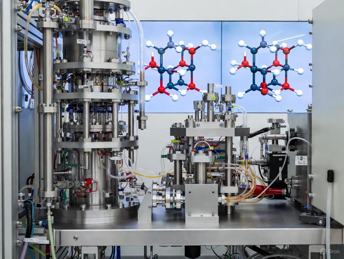
The power of contemporary MBE systems lies in the integration of multiple in-situ characterization techniques that provide real-time feedback during the growth process. This capability to monitor and adjust growth parameters without breaking vacuum has been transformative for synthesizing complex quantum materials with customized properties [10]. A typical modern MBE system integrates several key components and diagnostic tools, with the operational workflow illustrated in Figure 1.
Figure 1: Integrated MBE System with In-Situ Diagnostics. The diagram illustrates the key components of a modern MBE system, highlighting the integration of multiple characterization techniques that provide real-time feedback to the computer-controlled growth process.
The critical advancement in modern MBE has been the implementation of in-situ characterization techniques that allow direct observation of film growth processes without sample contamination. These techniques provide complementary information about the growing surface, enabling researchers to understand growth mechanisms and achieve precise control over epitaxial film properties [10]. The primary in-situ diagnostics employed in contemporary MBE systems include:
- Reflection High-Energy Electron Diffraction (RHEED): Provides real-time information on surface structure, morphology, and growth rate through oscillation monitoring [2] [10].
- Scanning Tunneling Microscopy (STM): Offers atomic-resolution imaging of surface topography and defect structures [10].
- X-ray Photoelectron Spectroscopy (XPS): Delivers chemical state analysis and compositional mapping of the growing surface [10].
- Spectroscopic Ellipsometry: Enables real-time monitoring of film thickness, roughness, and optical properties during growth [10].
The integration of these complementary techniques creates a powerful materials synthesis platform where growth parameters can be continuously adjusted based on real-time surface characterization, enabling the precise fabrication of complex quantum structures.
Research Reagent Solutions and Essential Materials
The synthesis of novel materials via MBE requires precisely controlled sources and substrates. Table 2 details the essential research reagents and their functions in MBE processes for quantum material synthesis.
Table 2: Essential Research Reagents for MBE Quantum Material Synthesis
| Material Category | Specific Examples | Function in MBE Process | Application in Quantum Materials |
|---|---|---|---|
| Elemental Sources | Gallium, Arsenic, Manganese, Bismuth, Tellurium [2] [8] | Provide fundamental constituents for film growth | GaAs semiconductors, MnBi₂Te₄ topological insulators |
| Complex Oxide Targets | Strontium, Niobium, Neodymium, Copper [9] [10] | Enable synthesis of complex oxide heterostructures | Superconducting cuprates, SrNbO₃, Sr₁₋ₓNdₓCuO₂ |
| Substrate Materials | GaAs, Ge, Si, Bulk-metal with TaN interlayer [2] [10] | Provide crystalline template for epitaxial growth | Nanowire integration on silicon, strain engineering |
| Dopant Sources | Silicon, Beryllium (p-type), Tin (n-type) [7] | Control electronic properties through intentional impurities | Precise tuning of carrier concentrations |
| Specialty Sources | Cracked arsenic, Oxygen radicals/ozone [2] [10] | Provide reactive species for compound formation | Oxide semiconductor growth, controlled stoichiometry |
The selection and control of these source materials is critical for achieving desired material properties. For instance, the use of cracked arsenic dimers (As₂) versus tetramers (As₄) significantly impacts incorporation efficiency during III-V semiconductor growth [10]. Similarly, specialized oxygen sources including radicals and ozone have been incorporated to achieve the desired oxidation states in multicomponent oxide films [2]. Recent advances have also explored surfactant-assisted growth, where impurities such as bismuth are used to improve surface mobility without incorporating into the crystal lattice, thereby enhancing crystalline quality [7].
Experimental Protocols for Quantum Material Synthesis
Protocol: Synthesis of Topological Insulator MnBi₂Te₄
The synthesis of intrinsic magnetic topological insulators represents an advanced application of MBE for quantum materials. The following protocol details the growth of MnBi₂Te₄ thin films, which combine topological surface states with long-range magnetic order [10] [8].
Materials and Equipment:
- Ultra-high vacuum MBE system (base pressure < 5×10⁻¹⁰ Torr)
- Bi (99.9999%), Mn (99.999%), and Te (99.9999%) effusion cells
- Epiready GaAs (111) or Si (111) substrates
- RHEED system for in-situ monitoring
- In-situ ARPES (angle-resolved photoemission spectroscopy) capability
Procedure:
- Substrate Preparation:
- Mount substrate on molybdenum sample holder using indium bonding.
- Transfer to MBE preparation chamber and heat to 300°C for 12 hours to desorb contaminants.
- Flash heat to 600°C (GaAs) or 900°C (Si) for 10 minutes to remove native oxide.
- Confirm (√3×√3)R30° surface reconstruction via RHEED for GaAs.
Growth Parameters:
- Set substrate temperature to 220-250°C.
- Calibrate beam equivalent pressures (BEP) using ion gauge:
- Bi: 2.0×10⁻⁷ Torr
- Mn: 1.5×10⁻⁸ Torr
- Te: 1.2×10⁻⁶ Torr
- Maintain BEP ratio Te:(Bi+Mn) ≈ 10-12 to prevent Te deficiency.
- Open all source shutters simultaneously to initiate growth.
- Grow at rate of 0.2-0.3 quintuple layers (QLs) per minute.
- Monitor RHEED intensity oscillations to track completion of each QL.
Post-growth Processing:
- Anneal at growth temperature for 10 minutes with Te flux only.
- Cool gradually to room temperature over 60 minutes under Te flux.
- Transfer in-situ to ARPES chamber for electronic structure characterization.
Quality Control:
- Confirm septuple-layer structure using RHEED oscillation periodicity.
- Verify magnetic properties using in-situ magneto-optical Kerr effect (if available).
- Check chemical composition using XPS with Ar⁺ sputtering depth profiling.
Protocol: Synthesis of Complex Oxide Heterostructures
Complex oxides exhibit a wide range of quantum phenomena including superconductivity, magnetism, and topological electronic states. This protocol outlines the growth of 4d and 5d oxide heterostructures using MBE [9].
Materials and Equipment:
- Oxide MBE system with high-pressure oxygen compatibility
- Metal sources: Sr, Nb, Nd (solid sources or e-beam evaporators)
- Oxygen plasma source or ozone generator
- Single-crystal SrTiO₃ (001) or LSAT substrates
- High-temperature substrate heater (up to 900°C)
- RHEED system with CCD camera for intensity monitoring
Procedure:
- Substrate Preparation:
- Etch SrTiO₃ substrates in buffered HF acid and anneal in oxygen.
- Transfer to MBE chamber and outgas at 600°C for 1 hour.
- Heat to 900-1000°C in 5×10⁻⁶ Torr oxygen for 30 minutes.
- Confirm atomically flat surface with sharp (1×1) RHEED pattern.
Growth Optimization:
- Set substrate temperature to 600-750°C depending on material.
- Use oxygen plasma source with pressure of 1×10⁻⁵ to 1×10⁻⁶ Torr.
- Calibrate metal fluxes using quartz crystal microbalance.
- Optimize metal/Oxygen flux ratio by monitoring RHEED oscillations.
- Grow at rate of 5-20 nm/hour depending on material complexity.
In-Situ Monitoring:
- Track layer-by-layer growth via RHEED intensity oscillations.
- Use spectroscopic ellipsometry for real-time stoichiometry control.
- For superlattices, alternate sources with shutter timing controlled by RHEED oscillations.
Post-growth Characterization:
- Perform in-situ XPS to verify oxidation states.
- Transfer under UHV to scanning probe microscopy for surface analysis.
- Measure transport properties using van der Pauw configuration.
Advanced Applications in Quantum Material Research
The precise control offered by MBE has enabled breakthroughs across multiple domains of quantum material research. The technique's capability to create atomically abrupt interfaces and complex heterostructures has proven particularly valuable for:
Topological Quantum Materials: MBE has enabled the synthesis of intrinsic magnetic topological insulators like MnBi₂Te₄, which provide platforms for realizing quantum anomalous Hall effect and axion insulators [10] [8]. These materials combine nontrivial band topology with long-range magnetic order, creating new phases of matter that could form the basis for topologically protected quantum computing.
Complex Oxide Heterostructures: Recent advances in MBE have produced breakthroughs in 4d and 5d oxide films and heterostructures that exhibit superconductivity, correlated electron physics, and topological electronic states [9]. The development of new MBE approaches for oxides has enabled the synthesis of ultra-high quality quantum materials with precisely controlled interfacial properties.
Nanostructured Quantum Materials: MBE techniques have been extended to create quantum nanostructures including nanowires with embedded quantum dots, enabling monolithical integration on silicon substrates for potential quantum communication and computing applications [2]. These nanostructures permit information processing and possible integration with on-chip applications, representing a significant advancement toward practical quantum devices.
The continued refinement of MBE, particularly through the integration of advanced in-situ diagnostics and machine learning-assisted growth control, promises to further expand the frontiers of quantum material synthesis, enabling the creation of increasingly sophisticated designer materials with customized electronic, magnetic, and optical properties.
Molecular Beam Epitaxy (MBE) is an advanced thin-film deposition technique enabling the synthesis of complex material structures with atomic-layer precision. This capability makes it indispensable for research on novel quantum materials, topological insulators, and high-temperature superconductors [11]. The MBE process occurs under ultra-high vacuum (UHV) conditions (typically 10⁻⁸–10⁻¹² Torr), where elemental or molecular beams condense on a heated crystalline substrate to form epitaxial layers with controlled composition and structure [2]. The exceptional control offered by MBE has facilitated breakthroughs across condensed matter physics, including the development of quantum wells, quantum dots, and heterostructure nanowire lasers [2].
This application note details the operational principles, selection criteria, and experimental protocols for three foundational MBE subsystems: effusion cells, shutters, and substrate heating. Mastery of these components is critical for researchers aiming to synthesize "designer materials" architected atom-by-atom for specific electronic, optical, or quantum functions [8].
Effusion Cells
Effusion cells, or Knudsen cells, are thermally controlled sources that generate precise, collimated beams of atoms or molecules for deposition. They are the primary method for delivering most elemental constituents in solid-source MBE.
- Operating Principle: High-purity source material is loaded into a crucible and heated to a specific temperature at which it sublimes or evaporates. The generated vapor effuses through a small aperture, creating a directed beam toward the substrate. The flux rate is governed by the vapor pressure of the material at the cell temperature [2].
- Key Design Considerations: Crucible material compatibility (typically Pyrolytic Boron Nitride, PBN), temperature uniformity, heater technology, and thermal stability are paramount for flux purity and reproducibility.
The table below summarizes the standard types of effusion cells and their typical applications based on operational temperature and material requirements.
Table 1: Classification and Specifications of Common MBE Effusion Cells
| Cell Type | Abbreviation | Typical Temperature Range | Common Applications |
|---|---|---|---|
| Low Temperature [12] [13] | NTEZ, LTEC | Up to 700°C | High vapor pressure materials (e.g., Cs, K, organic molecules) |
| Standard [12] [13] | WEZ, MTEC | 700°C – 1400°C | Common elements (e.g., Ga, Al, As) for III-V and II-VI semiconductors |
| High Temperature [12] [13] | HTEZ, HTS, HTEZ-W | Up to 2000°C | Low vapor pressure elements (e.g., Si, Ge, metals) |
| Production [12] [13] | PEZ | Varies | High-throughput systems requiring superior flux reproducibility and material utilization |
| Oxygen Resistant [12] [13] | OREZ | Varies | Oxide MBE for depositing materials like SrTiO₃ in high oxygen backgrounds [14] |
| Specialized Sources | SUSI, SUKO, DECO | Varies | Si sublimation, carbon doping, and P₂ generation via GaP decomposition, respectively [12] [13] |
Shutters
Shutters are mechanically actuated barriers positioned between the effusion cells and the substrate, providing digital control over the deposition process.
- Function: They enable the abrupt initiation and termination of atomic beams, allowing for the creation of sharp interfaces with monolayer accuracy. Computer-controlled shutter sequences are fundamental for growing complex layered structures like superlattices and quantum wells [2] [11].
- Design and Materials: Shutters must operate reliably in UHV and high-temperature environments. They are often designed for quick motion and long service life, with blades made from refractory metals such as molybdenum or tantalum to minimize reaction with stray fluxes and thermal deformation [15]. Modern shutter designs use magnetic coupling to transfer motion from the atmosphere into the UHV chamber, enhancing reliability over bellows-based systems [15].
Substrate Heating Systems
Substrate heaters provide precise and uniform thermal energy to the substrate, which is a critical parameter governing surface kinetics during epitaxial growth.
- Role in Epitaxy: The substrate temperature directly influences adatom surface mobility, desorption rates of contaminants and excess species, and chemical reaction rates between incorporating species. Optimal temperature is essential for achieving two-dimensional layer-by-layer growth and high crystalline quality [2] [11].
- Design Variants: Heaters employ resistive heating elements made from materials like tungsten, tantalum, graphite, or SiC. The choice of material depends on the required maximum temperature and the growth environment. For instance, SiC or noble metal heaters are used in oxide MBE where oxygen resistance is crucial [16]. Advanced designs incorporate flat serpentine filaments and efficient heat shielding to maximize temperature uniformity across the substrate while minimizing power consumption [14].
- Integration: Substrate heaters are typically integrated into a larger substrate manipulator, which also provides wafer rotation for deposition uniformity, electrical contacts for monitoring, and precise temperature measurement, often via a thermocouple [16] [17].
Experimental Protocols for Component Operation
Protocol: Effusion Cell Conditioning and Flux Calibration
This procedure ensures a stable, pure atomic flux from a newly installed or replenished effusion cell.
- Vacuum Check: Confirm the MBE growth chamber has reached base pressure (e.g., < 1×10⁻¹⁰ Torr).
- Cooling System: Verify that the cooling shroud surrounding the cell is active (typically with liquid nitrogen or chilled water) to prevent cross-contamination and protect UHV components [2].
- Outgassing:
- With the cell shutter closed, slowly ramp the cell temperature to a value ~50-100°C below its intended operating temperature.
- Hold at this temperature until the chamber pressure recovers to near its base level. This step drives off volatile contaminants from the source material and cell assembly.
- Flux Stabilization:
- Slowly increase the cell to its target operating temperature and open the shutter.
- Allow the beam equivalent pressure (BEP), as measured by an ion gauge, to stabilize. This may take from 30 minutes to several hours depending on the material.
- Flux Calibration:
Protocol: Atomic Layer-by-Layer Growth of Perovskite Oxides
This protocol outlines the shutter sequence for growing an oxide heterostructure, such as SrTiO₃, using an ALL-MBE approach with ozone as an oxidant [11].
- Substrate Preparation: Thermally clean a commercially available SrTiO₃ (001) substrate at ~600°C in UHV or in an oxygen/ozone flux to achieve an atomically flat, TiO₂-terminated surface.
- Temperature Setting: Set the substrate heater to the growth temperature, typically between 500°C and 700°C, as optimized for the specific material.
- Oxidant Introduction: Open the shutter of the ozone or oxygen gas source to establish a stable background pressure (e.g., 5×10⁻⁷ Torr).
- Shutter-Sequenced Deposition (for one SrTiO₃ unit cell):
- Sr Layer: Open the Sr effusion cell shutter for a pre-calibrated duration to deposit exactly one monolayer (ML) of Sr. Close the Sr shutter.
- Oxygen Soak: Maintain the substrate under the oxidant flux for 30-60 seconds to ensure oxidation of the Sr layer.
- Ti Layer: Open the Ti e-beam evaporator or effusion cell shutter to deposit exactly 1 ML of Ti. Close the Ti shutter.
- Oxygen Soak: Maintain the oxidant flux for another 30-60 seconds to fully oxidize the Ti layer, completing one unit cell of SrTiO₃.
- Cycle Repetition: Repeat Step 4 until the desired film thickness is achieved.
- In-situ Monitoring: Use RHEED to monitor the surface reconstruction and recovery of the diffraction pattern after each monolayer deposition, which confirms layer-by-layer growth [11].
Protocol: Substrate Temperature Calibration
Accurate substrate temperature measurement is non-trivial in MBE. This protocol describes common calibration methods.
- Thermocouple Correlation: The manipulator's thermocouple reading is an initial reference but may not reflect the actual wafer surface temperature.
- Material-Dependent Calibration Points:
- Melting Point Observance: Observe the melting of small pieces of pure elements (e.g., In, Sn, Al) placed on a dummy substrate. The temperature reading at which melting occurs provides a fixed point for calibration.
- Surface Phase Transitions: For common substrates like Si or GaAs, the temperature at which specific surface reconstructions occur (observable via RHEED) is well-known and can be used as a calibration point (e.g., the (7×7) to (1×1) transition on Si(111) at ~860°C).
- Pyrometer Use: An infrared pyrometer can measure surface temperature directly but requires knowledge of the material's emissivity, which can change with temperature and surface roughness.
System Integration and Workflow
The coordinated operation of effusion cells, shutters, and substrate heaters is what enables atomic-precision synthesis. The following diagram illustrates the logical workflow and information flow between these core components during a standard MBE growth run.
The Researcher's Toolkit: Essential MBE Materials and Reagents
Successful MBE synthesis relies on ultra-high-purity source materials and specialized consumables. The following table catalogs key items required for establishing and maintaining an MBE system.
Table 2: Essential Research Reagents and Materials for MBE Systems
| Item Name | Function / Application | Critical Specifications |
|---|---|---|
| Effusion Cell Crucibles [12] [17] | Holds source material; must be inert at high temperatures. | Material (e.g., PBN, Al₂O₃, Graphite), volume (e.g., 35-500 cc) |
| Ultra-Pure Elemental Sources (e.g., Ga, As, Si) [2] | Provide the atomic beams for film constituents. | Purity (typically ≥ 99.9999% or 6N), form (lump, wire, chip) |
| Thermocouples (Type-C: W/Re) [17] | Measure effusion cell and substrate temperatures. | Type, sheath material, temperature range |
| Substrate Mounting Kit | Secures the wafer to the heater/manipulator for good thermal contact. | Indium-free holders [18], high-temperature adhesives (e.g., UHV-compatible silver paint) |
| Cryogenic Coolants [2] | Chills cryopanels/cryopumps to trap impurities and maintain UHV. | Liquid Nitrogen (LN₂), Cold Nitrogen Gas |
| Oxidant Gas Sources [11] | Provides reactive oxygen species for oxide film growth. | Ozone (O₃), RF-plasma generated atomic oxygen, purity ≥ 99.995% |
| Shutter Blades [15] | Intercepts atomic beams; requires periodic cleaning/replacement. | Material (Molybdenum, Tantalum), shape/dimensions |
| RHEED Filaments | Electron source for in-situ growth monitoring. | Standard replacement part for RHEED electron gun |
The Critical Role of RHEED for Real-Time Growth Monitoring
Molecular Beam Epitaxy (MBE) is an ultra-high vacuum technique for depositing single-crystal thin films with atomic-layer precision. Its development was profoundly advanced by the integration of Reflection High-Energy Electron Diffraction (RHEED), which provides unparalleled, real-time insight into surface crystallography during growth [2]. The compatibility of RHEED's grazing-incidence geometry with the MBE deposition process makes it an indispensable in-situ diagnostic tool. Unlike characterization methods that probe the bulk material, RHEED is exceptionally surface-sensitive, gathering information primarily from the outermost atomic layers of the sample [19]. This capability allows researchers to monitor dynamic surface processes, including growth rates, surface roughness, and reconstruction, with monolayer accuracy, enabling the synthesis of complex quantum nanostructures that are critical for advanced electronic and photonic devices [2] [20].
Technical Principles of RHEED
System Configuration and Operational Mechanics
A basic RHEED system consists of three core components: an electron gun, the sample, and a phosphorescent detector screen [19]. The electron gun generates a beam of high-energy electrons (typically in the 10-30 keV range) that is directed towards the sample at a very shallow glancing angle (often 1-2 degrees) [19] [21]. This shallow angle is the key to its surface sensitivity, as it limits the penetration depth of the electrons into the material, ensuring that the resulting diffraction pattern originates almost exclusively from the surface atoms [21]. The diffracted electrons interfere constructively at specific angles and strike a phosphor screen, creating a visible diffraction pattern that is a direct function of the atomic arrangement on the sample surface [19]. Modern systems are often equipped with charge-coupled device (CCD) cameras to capture these patterns for digital analysis [19].
Diffraction Pattern Analysis and the Ewald Sphere Construction
The interpretation of RHEED patterns relies on understanding the wave-like properties of electrons and their interaction with the crystalline surface. When the electron beam strikes the surface, atoms diffract the incident electrons. These diffracted waves interfere constructively at specific angles determined by the surface crystal structure and the electrons' wavelength, forming the characteristic pattern on the detector [19].
The theoretical analysis is commonly visualized using the Ewald sphere construction [22]. In this model, the reciprocal lattice of a crystal surface is represented not as a set of points (as in 3D crystals), but as a series of infinite reciprocal lattice rods extending perpendicular to the surface. This is due to the minimal periodicity in the direction normal to the surface [19]. The Ewald sphere, with a radius proportional to the wavevector of the incident electron beam, is constructed centered on the crystal surface. The points where this sphere intersects the reciprocal lattice rods satisfy the diffraction condition, and each intersection corresponds to a diffracted beam (e.g., the (00) or specular beam) that appears as a feature on the RHEED pattern [19] [22]. The geometry and intensity of these features encode rich information about the surface.
Table 1: Key Parameters in a Typical RHEED System
| Component/Parameter | Typical Specification | Function and Impact |
|---|---|---|
| Electron Gun Energy | 10–30 keV | Determines electron wavelength and penetration depth. Higher energy provides more pattern information but can reduce surface sensitivity at larger angles [19]. |
| Incident Angle (Glancing) | 1–2 degrees | Critical for surface sensitivity. Minimizes electron penetration into the bulk, ensuring the signal originates from the top few atomic layers [21]. |
| Electron Source | Tungsten Filament | Common cathode material due to its low work function, facilitating electron emission [19]. |
| Detector | Phospholuminescent Screen + CCD Camera | Converts the diffracted electron signal into a visible pattern for observation and digital recording [19]. |
| Vacuum Environment | Ultra-High Vacuum (UHV) | Standard operating environment of MBE, necessary to prevent scattering of the electron beam by gas molecules and to maintain a clean surface [2]. |
Practical Applications and Protocols for Real-Time Monitoring
Calibration of Growth Rates via RHEED Oscillations
One of the most powerful quantitative applications of RHEED is the calibration of deposition rates using RHEED intensity oscillations [2]. This technique is foundational for the growth of complex heterostructures. The protocol involves initiating growth on a perfectly flat, atomically smooth substrate surface. Under these conditions, the intensity of the specular beam (the (00) spot) in the RHEED pattern begins to oscillate with a period corresponding exactly to the time required to deposit a single atomic monolayer [2]. The oscillation occurs because the surface roughness, and hence the diffuse scattering of electrons, changes in a periodic manner as islands form, coalesce, and are subsequently covered by the next layer.
Standard Protocol for Flux Calibration:
- Substrate Preparation: Begin with a substrate (e.g., GaAs) that has been prepared to have an atomically smooth, (2x4) reconstructed surface, as confirmed by a sharp, streaky RHEED pattern.
- Growth Initiation: Close the shutter of the source cell (e.g., Ga) and stabilize the cell temperature to achieve the desired flux. Simultaneously, open the shutter of the group-V element (e.g., As) to stabilize the surface.
- Data Acquisition: Position the RHEED beam on a specific crystal azimuth and monitor the intensity of the specular spot with a photomultiplier tube or CCD camera. Open the shutter of the source cell to initiate growth. Record the intensity of the specular spot versus time.
- Analysis: Count the number of oscillations (intensity maxima or minima) over a known time interval. The growth rate per hour is calculated as: (Number of Oscillations × Monolayer Height × 3600) / (Time in Seconds). This provides a direct, in-situ measurement of the deposition flux from the source [2].
Assessment of Surface Morphology and Reconstruction
RHEED patterns provide immediate qualitative feedback on the morphology of the growing surface, which is critical for achieving high-quality material.
- Streaky Patterns: Indicate a smooth, two-dimensional (2D) layer-by-layer growth morphology. The streaks arise from a partial relaxation of the crystal truncation rods due to a perfectly flat surface with limited coherence length [21].
- Spotty Patterns: Are characteristic of a rough, three-dimensional (3D) island growth mode. The spots indicate that the electron beam is being transmitted through and diffracted from discrete islands on the surface [21].
- Reconstructed Patterns: The presence of additional streaks or spots between the fundamental bulk streaks signifies a surface reconstruction, where the atoms at the surface rearrange into a periodic structure different from the bulk crystal to minimize their energy. Analyzing the spacing and arrangement of these features reveals the specific reconstruction type (e.g., (2x4) or c(4x4) for GaAs) [20].
The following diagram illustrates the experimental workflow from electron diffraction to morphological interpretation:
Advanced Application: Monitoring Complex Oxides and Alloys
RHEED's utility extends beyond conventional III-V semiconductors. It is equally critical for monitoring the growth of complex oxides and alloys. For instance, during the growth of Si and SiGe alloys from molecular beams of Si₂H₆ and GeH₄, in-situ measurement of the growth rate on a monolayer basis can provide detailed chemical information about surface processes like reaction and segregation [23]. The protocol involves monitoring changes in the RHEED pattern and oscillation frequency as the composition or material is changed, allowing researchers to deduce chemical kinetics and segregation coefficients in real time.
The Researcher's Toolkit: Essential RHEED Components
Table 2: Essential Components and Materials for RHEED Monitoring
| Item | Function and Importance |
|---|---|
| High-Energy Electron Gun | Generates the primary electron beam (typically 10-30 keV). Tungsten filaments are a common electron source. The gun's energy and focus determine the resolution and information content of the diffraction pattern [19]. |
| UHV-Compatible Manipulator | Holds the sample and allows for precise manipulation, including heating, cooling, and rotation around axes perpendicular (azimuthal control) and parallel to the surface. Azimuthal rotation is essential for probing different crystal directions and optimizing pattern intensity [19]. |
| Phosphor Screen Detector | A phospholuminescent screen that converts the impinging diffracted electrons into visible light, forming the diffraction pattern for direct observation [19]. |
| CCD Camera & Software | Captures the diffraction pattern and specular spot intensity in real time for digital analysis, storage, and quantification (e.g., measuring RHEED oscillations) [19] [20]. |
| Ultra-High Vacuum (UHV) System | A necessity for both MBE and RHEED. Maintains a clean, contamination-free sample surface and prevents scattering of the electron beam by residual gas molecules [2]. |
| Effusion Cells/Crucibles | MBE sources that contain ultra-pure elements (e.g., Ga, As, Al). Their temperature-controlled shutters enable the precise atomic-layer deposition that RHEED monitors [2]. |
Visualization of RHEED Intensity Oscillations
The following diagram outlines the logical relationship between surface morphology and the resulting RHEED intensity oscillations, which are central to quantitative growth monitoring:
Core Principles and Advantages of Molecular Beam Epitaxy
Molecular-beam epitaxy (MBE) is an epitaxial deposition technique for creating high-purity, single-crystal thin films one atomic layer at a time. This process occurs in an ultra-high vacuum (UHV) environment, typically at pressures between 10⁻⁸ to 10⁻¹² Torr, which is fundamental to achieving its signature characteristic: ultra-pure films with minimal contamination [2] [1]. The deposition rate is deliberately slow, often less than 3,000 nm per hour, to facilitate epitaxial growth and allow for precise monolayer control [2] [1].
A key technological differentiator of MBE is the use of computer-controlled shutters in front of individual effusion cells. Each cell contains an ultra-pure source material, such as gallium or arsenic, which is heated until it sublimes, creating a directional beam of atoms or molecules [2] [1]. These shutters can be opened and closed in sequence, enabling the fabrication of intricate heterostructures—stacks of different semiconductor materials—with atomically sharp interfaces [2]. This capability is crucial for modern semiconductor devices, as it allows engineers to confine electrons in quantum wells or quantum dots, radically altering the electronic and optical properties of the material [2].
Table 1: Fundamental Characteristics of the MBE Process
| Feature | Specification/Description | Primary Advantage |
|---|---|---|
| Operating Environment | Ultra-High Vacuum (UHV), 10⁻⁸ – 10⁻¹² Torr | Minimizes contamination, enabling ultra-pure film growth [2] [1]. |
| Deposition Rate | Typically < 3,000 nm per hour | Allows for epitaxial growth and precise monolayer control [2] [1]. |
| In-situ Monitoring | Reflection High-Energy Electron Diffraction (RHEED) | Provides real-time feedback on crystal layer growth and surface quality [2]. |
| Composition Control | Multiple effusion cells with computer-controlled shutters | Enables fabrication of complex heterostructures and doping profiles [2]. |
Application Protocols: MBE for Advanced Material Synthesis
The unparalleled control offered by MBE makes it a cornerstone technique for synthesizing novel quantum materials and two-dimensional systems. The following protocols detail specific methodologies for growing two such materials: stanene and complex oxides.
Protocol 1: MBE Growth of Few-Layer Stanene
Stanene, a two-dimensional topological material composed of a single layer of tin atoms in a honeycomb lattice, is a promising candidate for room-temperature quantum spin Hall insulators [24]. Its growth is highly sensitive to the substrate, which acts as a template and influences the stanene's electronic structure.
Substrate Preparation:
- Bi₂Te₃(111): A topological insulator substrate. The substrate is used at room temperature [24].
- PbTe(111): An insulating semiconductor substrate with a lattice constant close to that of stanene. A two-step growth recipe is employed [24].
- InSb(111): A semiconductor substrate. It must be terminated with Sb prior to growth [24].
- Cu(111): A metal substrate. Requires low-temperature MBE technique to form extremely flat, unbuckled stanene [24].
Growth Procedure (Two-Step Method for PbTe substrate):
- Low-Temperature Deposition: Deposit high-purity Sn (99.9999%) atoms from an effusion cell onto the PbTe(111) substrate held at approximately 150 K [24].
- Post-Deposition Annealing: Anneal the deposited film by raising the substrate temperature from 150 K to approximately 400 K. This step improves the crystalline quality and morphology of the stanene film [24].
Characterization and Analysis:
- In-situ Scanning Tunneling Microscopy (STM): Used for atomic-resolution imaging to confirm the hexagonal arrangement of Sn atoms and measure surface morphology [24].
- Angle-Resolved Photoemission Spectroscopy (ARPES): Measures the electronic band structure, identifying key features like band gaps and topological edge states [24].
- Transport Measurements: Performed at cryogenic temperatures (e.g., down to sub-kelvin) to investigate properties like superconductivity and its behavior under high magnetic fields [24].
Protocol 2: Hybrid MBE for Complex Oxide Synthesis
Hybrid MBE (hMBE) is an advanced variant that combines traditional solid-source effusion cells with gas-source delivery of metal-organic precursors [25] [6] [26]. This method is particularly powerful for the atomically precise synthesis of complex oxide materials, such as perovskite oxides and rutile-based quantum materials, where controlling the stoichiometry of volatile or highly reactive metals is challenging [25] [6].
System Configuration:
- Integrate a metal-organic precursor injection system into a standard UHV MBE chamber.
- Maintain independent temperature control for traditional effusion cells and the substrate heater.
- Use an all-metal UHV construction to ensure high purity and minimize contamination [26].
Growth Procedure for BaTiO₃ or Similar Perovskites:
- Precursor Delivery: Introduce a metal-organic precursor (e.g., Titanium Tetraisopropoxide) via a controlled gas injection system. Simultaneously, evaporate a solid source (e.g., Ba) from a standard effusion cell [25] [26].
- Flux Control: Precisely regulate the fluxes of the metal-organic precursor and the solid source to achieve the desired metal cation ratio (Ba:Ti = 1:1) at the substrate surface.
- Oxidation: Direct an oxidant (e.g., purified oxygen or an oxygen plasma) onto the heated substrate to facilitate the formation of the oxide crystal lattice [2] [1].
- In-situ Monitoring: Use RHEED to monitor the growth in real-time, observing oscillations in the diffraction pattern to confirm layer-by-layer growth [2].
Key Advantages of hMBE:
- Superior Stoichiometry Control: The gas-source delivery allows for more precise control over the incorporation of difficult-to-handle elements, leading to perfect cation stoichiometry [25] [6].
- Reduced Defects: Excellent stoichiometric control directly translates to a lower density of point defects (e.g., vacancies) in the final film [6].
- Strain and Interface Engineering: This level of control enables the use of dimensionality, strain, and heterointerfaces as knobs to probe and tailor material properties [25].
Quantitative MBE Advantages in Research and Development
The superiority of MBE is demonstrated through quantifiable metrics in material purity, interface control, and electronic performance. The table below summarizes key comparative data from research applications.
Table 2: Quantitative Performance of MBE-grown Materials in R&D
| Material System | Key Metric | MBE Performance | Context & Significance |
|---|---|---|---|
| GeSn Alloys [27] | Sn-Sn 1st Nearest Neighbor (1NN) Short-Range Order | ~15% stronger preference for Sn-Sn 1NN vs. CVD | Indicates different growth kinetics; can be tuned via surface termination to engineer band structure [27]. |
| Stanene on PbTe(111) [24] | Superconducting Critical Temperature (T_c) | Tunable with film thickness | Demonstrates ability to create Tc-tunable superconducting systems from a non-superconducting element [24]. |
| GaAs/AlGaAs Heterostructures [1] | 2D Electron Gas (2DEG) Mobility | High mobility achieved | Essential for high-performance transistors in communication and microwave technologies [1]. |
| General MBE Films [2] [1] | Defect Density / Purity | Exceptionally low | Result of UHV environment and absence of carrier gases; critical for optical device efficiency and quantum phenomena [2] [1]. |
| Oxide Heterostructures [25] [6] | Stoichiometric Control | Atomic-level precision | Enabled by hybrid MBE; allows stabilization of metastable phases and defect-engineered films [25] [6]. |
The Scientist's Toolkit: Essential Research Reagent Solutions
Successful MBE research relies on a suite of specialized sources and substrates. The following table details key materials and their functions.
Table 3: Essential Materials for MBE Research
| Item / Reagent | Function in the MBE Process |
|---|---|
| Ultra-High Purity Elements (e.g., Ga, As, Sn >99.9999%) | Source material in effusion cells; high purity is mandatory to prevent unintentional doping and defects [2] [24]. |
| Metal-Organic Precursors (for hMBE) | Gas-source for incorporating metals (e.g., Ti, Sr); enables superior stoichiometric control for complex oxides [25] [26]. |
| Single-Crystal Substrates (e.g., GaAs, Si, SrTiO₃) | Provides the crystalline template for epitaxial growth; lattice mismatch with the film is a critical design parameter [2] [24]. |
| Oxidant Sources (e.g., O₂, Ozone, Oxygen Plasma) | Reactive species for the growth of oxide materials; used to achieve the desired oxidation state in multicomponent oxides [2] [1]. |
Advanced MBE Methodologies and Their Transformative Applications in Quantum Materials
Molecular Beam Epitaxy (MBE) has long been the benchmark technique for synthesizing high-purity crystalline thin films with atomic-scale precision. Recent innovations have dramatically expanded its capabilities beyond traditional boundaries, enabling the fabrication of ultra-pure, defect-engineered films and the stabilization of metastable phases previously considered unattainable [6]. These advancements are particularly crucial for complex oxides and quantum materials, where precise control over composition and structure at the atomic level is essential for unlocking novel electronic, magnetic, and quantum properties [6] [8]. This document provides application notes and detailed experimental protocols for three cutting-edge MBE methodologies: Hybrid MBE, Suboxide MBE, and Thermal Laser Epitaxy, framing them within the broader context of novel material synthesis research.
The evolution of MBE is driven by the increasing demands of next-generation technologies. From quantum computing and spintronics to advanced optoelectronics and power electronics, these applications require materials with precisely engineered properties that can only be achieved through atomic-level control during synthesis [6] [28]. The techniques discussed herein address fundamental challenges in the growth of complex materials, particularly those involving elements with high vapor pressures, complex oxidation states, or difficult-to-control stoichiometries. By bridging the gap between synthesis science and source chemistry, these methods provide a guiding framework for future innovations in materials discovery [29].
Hybrid Molecular Beam Epitaxy (Hybrid MBE)
Principles and Applications
Hybrid MBE combines conventional elemental solid sources with metalorganic gaseous precursors to achieve enhanced control over stoichiometry, particularly for oxide materials where traditional MBE faces challenges with volatile elements or complex cation ratios. This technique has proven exceptionally valuable for growing perovskite oxides, wide bandgap semiconductors, and complex oxide heterostructures that are fundamental to next-generation electronics [6] [30]. The metalorganic precursors (typically β-diketonates or alkoxides) provide a steady, controllable flux of metal cations that can be precisely regulated using pressure-based flow controllers, offering significant advantages over traditional effusion cells for elements with low vapor pressures or high melting points.
The "hybrid" approach specifically addresses the challenge of cation oxidation and incorporation, leading to superior film quality with reduced defect densities. For instance, in the growth of SrTiO₃, using a titanium metalorganic precursor (such as tetrakis(diethylamido)titanium or titanium tetraisopropoxide) alongside a conventional strontium effusion cell and an oxygen plasma source enables optimal stoichiometric control with exceptional crystalline perfection [30]. This method has enabled the synthesis of complex oxides with unprecedented electron mobility, such as SrSnO₃ films with room-temperature conductivity exceeding 10⁴ S cm⁻¹ [30]. The technique is particularly advantageous for achieving precise cation stoichiometry in multi-component oxides, where traditional MBE often struggles with phase purity and defect control.
Quantitative Growth Parameters for Selected Materials
Table 1: Hybrid MBE Growth Parameters for Selected Oxide Materials
| Material | Metalorganic Precursor | Growth Temperature (°C) | Oxidant | Key Achieved Properties |
|---|---|---|---|---|
| SrTiO₃ | Titanium tetraisopropoxide | 700-900 | O₂ plasma or O₃ | High electron mobility, low defect density [30] |
| BaSnO₃ | Tin tetra-tert-butoxide | 700-900 | O₂ plasma | Room-temperature conductivity >10⁴ S cm⁻¹ [30] |
| GdTiO₃ | Titanium tetraisopropoxide | 650-800 | O₂ plasma | Metallic conductivity, magnetic ordering [30] |
| SrVO₃ | Vanadium oxytriisopropoxide | 500-700 | O₂ plasma | High conductivity bottom electrode [30] |
Experimental Protocol: Growth of High-Mobility BaSnO₃ Films
Research Reagent Solutions and Essential Materials:
Table 2: Key Research Reagents for Hybrid MBE of BaSnO₃
| Reagent/Material | Function | Specifications & Handling |
|---|---|---|
| Tin tetra-tert-butoxide | Tin precursor | High-purity (99.99%), maintained at 45-55°C for optimal vapor pressure |
| Barium metal | Barium source | High-purity (99.99%) in effusion cell, operated at 500-600°C |
| Oxygen gas | Oxidant | Research grade (99.999%), fed into RF plasma source |
| Single crystal substrate | Template for epitaxy | (001) SrTiO₃ or (001) MgO, chemically etched and annealed |
| RF plasma source | Oxygen radical generation | 300-500W forward power, operating pressure <5×10⁻⁶ Torr |
Step-by-Step Procedure:
Substrate Preparation: Thermally etch SrTiO₃ (001) substrate at 950°C for 30 minutes in oxygen pressure of 5×10⁻⁵ Torr, confirming a TiO₂-terminated surface with sharp (1×1) Reflection High-Energy Electron Diffraction (RHEED) pattern.
Source Preparation and Calibration:
- Load barium into a high-temperature effusion cell and outgas at 800°C for 2 hours prior to growth.
- Install tin tetra-tert-butoxide in a stainless-steel bubbler maintained at 50°C using a precision temperature controller.
- Calibrate tin precursor flux using a quartz crystal microbalance at the substrate position, establishing a precise relationship between bubbler pressure and deposition rate.
Growth Process:
- Stabilize substrate temperature at 750°C under ultra-high vacuum (UHV) conditions (<1×10⁻⁹ Torr).
- Initiate oxygen flow to the plasma source, maintaining a chamber pressure of 5×10⁻⁶ Torr with plasma power of 350W.
- Open shutters for barium effusion cell and tin precursor simultaneously to initiate growth.
- Maintain Ba:Sn flux ratio of approximately 1:1 as determined by pre-calibration, monitoring RHEED pattern for layer-by-layer growth.
- Grow to desired thickness (typically 20-100 nm), observing periodic RHEED intensity oscillations to confirm two-dimensional growth.
Post-Growth Processing:
- After closing precursor shutters, anneal the film in oxygen plasma for 10 minutes at growth temperature.
- Cool the sample slowly (5°C/minute) to room temperature under UHV conditions.
- Perform in-situ RHEED and X-ray Photoelectron Spectroscopy (XPS) to assess surface structure and composition before removing from UHV environment.
Troubleshooting Notes:
- If RHEED oscillations dampen quickly, reduce growth rate or slightly increase substrate temperature.
- If film becomes insulating, check oxygen plasma stability and increase oxidant flux slightly.
- For rough surface morphology, verify precursor flux stability and ensure optimal substrate termination.
Hybrid MBE Reaction Pathway
Diagram 1: Hybrid MBE reaction pathway for metalorganic precursors
Suboxide Molecular Beam Epitaxy (Suboxide MBE)
Principles and Applications
Suboxide MBE represents a paradigm shift in the growth kinetics of III-O and IV-O materials, explicitly addressing the fundamental challenge of volatile suboxide formation that limits the growth of many oxide materials [31] [32]. This technique leverages the controlled supply of pre-formed suboxide molecules (e.g., Ga₂O, In₂O, SnO) as the primary cation delivery species, rather than elemental metals, fundamentally altering the reaction pathway and enabling access to previously inaccessible growth regimes [31]. The method directly addresses the complex 2-step kinetics that govern the MBE growth of many oxide materials, where the formation and desorption of volatile suboxides traditionally limits growth rates and film quality.
In conventional MBE of oxides, the reaction of elemental metals with oxygen follows a two-step process where metal atoms first form volatile suboxides, which then either incorporate into the film or desorb, creating a significant limitation in growth efficiency [31]. Suboxide MBE bypasses this limitation by directly supplying the suboxide molecules, effectively shifting the growth from a reaction-limited to a supply-limited regime. This approach dramatically expands the "film growth window" (FGW) - the range of conditions under which high-quality films can be grown - particularly at higher temperatures where traditional MBE fails due to excessive suboxide desorption [31]. The technique has proven particularly valuable for growing high-purity β-Ga₂O₃, In₂O₃, SnO₂, and related alloys, which are crucial for power electronics, transparent conductors, and gas sensing applications.
Quantitative Growth Windows and Kinetics
Table 3: Suboxide Formation and Film Growth Windows for Selected Materials
| Material | Volatile Suboxide | Suboxide Formation Window (SFW) | Film Growth Window (FGW) | Optimal Growth Temperature |
|---|---|---|---|---|
| β-Ga₂O₃ | Ga₂O | Wide (κ ≥ K) | Expands with temperature [31] | 500-700°C [31] |
| In₂O₃ | In₂O | Wide (κ ≥ K) | Limited by In₂O desorption [31] | 450-650°C [31] |
| SnO₂ | SnO | Wide (κ ≥ K) | Limited at high temperature [31] | 500-700°C [31] |
| Ga₂Se₃ | Ga₂Se | Similar to oxides [31] | Similar to oxides [31] | 400-600°C [31] |
Experimental Protocol: Growth of β-Ga₂O₃ via Suboxide MBE
Research Reagent Solutions and Essential Materials:
Table 4: Key Research Reagents for Suboxide MBE of β-Ga₂O₃
| Reagent/Material | Function | Specifications & Handling |
|---|---|---|
| Gallium metal | Gallium source for suboxide generation | 99.9999% purity, loaded in low-temperature effusion cell |
| Ga₂O powder | Alternative direct suboxide source | High-purity synthesized powder, loaded in dedicated cell |
| Oxygen gas | Oxidant | Research grade (99.999%), precise pressure control critical |
| Substrate | Template for epitaxy | (010) β-Ga₂O₃ single crystal, solvent cleaned |
| RF plasma source | Active oxygen generation | Optimized for high radical yield |
Step-by-Step Procedure:
Suboxide Source Setup:
- Option A (In-situ suboxide generation): Configure separate effusion cells for gallium and gallium oxide (Ga₂O), with the Ga₂O cell temperature calibrated to provide controlled suboxide flux.
- Option B (Direct suboxide delivery): Use a single high-temperature effusion cell containing pre-synthesized Ga₂O, operated at 700-800°C to generate molecular Ga₂O flux.
- Calibrate suboxide flux using a quartz crystal microbalance and confirm composition via mass spectrometry.
Substrate Preparation:
- Clean β-Ga₂O₃ (010) substrates using organic solvents followed by oxygen plasma cleaning.
- Load into MBE system and anneal at 900°C in UHV for 30 minutes to remove surface contaminants.
- Confirm surface quality using sharp RHEED patterns before initiating growth.
Growth Process:
- Stabilize substrate at target growth temperature (550-650°C).
- For in-situ suboxide generation: Open gallium and gallium oxide effusion cells simultaneously, with cell temperatures calibrated to produce stoichiometric Ga₂O flux.
- Initiate oxygen plasma with careful pressure control (1×10⁻⁶ to 1×10⁻⁵ Torr).
- Monitor growth via RHEED to confirm epitaxial relationship.
- Optimize metal-to-oxygen flux ratio (R = ϕGa/ϕO) to operate within the Film Growth Window, typically at slightly metal-rich conditions.
Real-time Monitoring and Optimization:
- Track RHEED intensity oscillations to monitor growth rate and mode.
- Use mass spectrometry to monitor desorbing species and adjust fluxes to minimize Ga₂O desorption.
- For doped films, introduce dopant sources (Sn for n-type, Mg for semi-insulating) with calibrated fluxes.
Post-Growth Processing:
- Anneal film in oxygen environment at growth temperature for 10 minutes to address oxygen vacancies.
- Cool slowly (3-5°C/minute) under UHV to room temperature.
- Perform in-situ characterization including XPS and AFM before removal from UHV.
Troubleshooting Notes:
- If growth rate decreases unexpectedly, check suboxide source stability and replenish if necessary.
- If RHEED pattern becomes spotty, reduce growth rate or slightly increase substrate temperature.
- For conductive films requiring high electron mobility, ensure slightly reducing conditions during growth.
Suboxide MBE Kinetic Pathway
Diagram 2: Comparison of traditional MBE limitations vs. suboxide MBE pathway
Thermal Laser Epitaxy (TLE)
Principles and Applications
Thermal Laser Epitaxy (TLE) represents a revolutionary approach to thin film synthesis that combines precise thermal control from laser heating with the atomic-level precision of conventional MBE [6] [30]. This hybrid technique enables the growth of materials at temperatures and under conditions that are inaccessible by conventional resistive heating methods, particularly advantageous for thermally sensitive substrates, metastable phases, and materials with large thermal mismatches. The focused energy delivery of laser heating allows for extreme thermal gradients and rapid heating/cooling cycles that can fundamentally alter growth kinetics and enable novel phase formation.
TLE is particularly valuable for growing complex carbon-based materials, high-temperature superconductors, and materials requiring extreme synthesis conditions [30]. The localized heating prevents interdiffusion at substrate-film interfaces and enables the use of temperature-sensitive substrates. Additionally, the rapid thermal cycling possible with TLE can suppress the formation of thermodynamically stable but undesirable phases, allowing for the stabilization of metastable structures with unique properties. This technique has opened new pathways for materials discovery beyond the constraints of conventional thermal budgets.
Experimental Protocol: TLE of Carbon Films
Research Reagent Solutions and Essential Materials:
Table 5: Key Research Reagents for Thermal Laser Epitaxy
| Reagent/Material | Function | Specifications & Handling |
|---|---|---|
| Laser system | Precise thermal control | Fiber-coupled diode laser (808-980nm), uniform beam profile |
| Carbon source | Film precursor | High-purity graphite e-beam target or gaseous hydrocarbon |
| Substrate | Template for epitaxy | Single crystal wafer with laser-transparent properties |
| Beam delivery | Laser guidance | Optical fibers with UHV-compatible viewport |
| Pyrometer | Temperature monitoring | Non-contact, calibrated for substrate material |
Step-by-Step Procedure:
System Configuration:
- Integrate fiber-coupled laser system with UHV-compatible optical viewport aligned for normal incidence on substrate.
- Calibrate laser power distribution across substrate surface using thermal imaging.
- Install non-contact pyrometer for real-time temperature monitoring and feedback control.
Substrate Preparation and Loading:
- Select appropriate substrate (e.g., sapphire, SiC, or MgO) based on optical absorption properties at laser wavelength.
- Clean substrate using standard semiconductor cleaning procedures.
- Mount substrate on specially designed holder that minimizes thermal mass while ensuring mechanical stability.
Growth Process:
- Pump system to UHV base pressure (<1×10⁻⁹ Torr).
- Initiate laser heating with rapid thermal ramp (up to 500°C/s) to target growth temperature (600-1200°C, material-dependent).
- Once thermal stability achieved, open shutter for carbon source (e-beam evaporation of graphite or introduction of hydrocarbon gas).
- Monitor growth in real-time using RHEED, adjusting laser power dynamically to maintain constant temperature despite changing surface emissivity.
- For complex heterostructures, implement rapid thermal cycling between layers to minimize interdiffusion.
Advanced Process Control:
- Implement closed-loop temperature control using pyrometer feedback to laser power supply.
- Use multi-zone laser heating for improved temperature uniformity across substrate.
- For patterned growth, implement laser scanning with spatial light modulators for site-specific deposition.
Post-Growth Analysis:
- Characterize film quality using in-situ techniques including XPS, LEED, and STM.
- Perform ex-situ structural characterization (XRD, Raman spectroscopy) and electrical measurements.
Troubleshooting Notes:
- If temperature fluctuations occur, check pyrometer alignment and calibrate against substrate-specific emissivity.
- For non-uniform growth, characterize laser beam profile and implement beam homogenization if necessary.
- If film stress causes delamination, optimize heating/cooling rates to minimize thermal mismatch.
Thermal Laser Epitaxy System Configuration
Diagram 3: Thermal laser epitaxy system configuration
Integrated Workflow for Advanced Material Synthesis
Material Discovery and Optimization Pipeline
The advanced MBE techniques described herein are most powerful when integrated into a comprehensive materials discovery pipeline, such as those implemented at national user facilities like PARADIM (Platform for the Accelerated Realization, Analysis, and Discovery of Interface Materials) [33]. These facilities combine state-of-the-art synthesis capabilities with advanced characterization and data science approaches to accelerate the development of new quantum materials and heterostructures. The integration of AI and machine learning with MBE growth is particularly transformative, enabling real-time process optimization and predictive modeling of growth outcomes [28].
A key advantage of these advanced MBE techniques is their compatibility with in-situ characterization methods that provide real-time feedback on growth quality and mechanism. Techniques including RHEED, XPS, and mass spectrometry can be directly integrated into the growth environment, providing immediate insights into growth kinetics and enabling dynamic adjustment of parameters [33]. Furthermore, the connection of these synthesis tools to world-class characterization facilities, such as atomically-resolved scanning transmission electron microscopy (STEM) and angle-resolved photoemission spectroscopy (ARPES), creates a closed-loop feedback system for materials optimization [33].
Advanced MBE Integrated Workflow
Diagram 4: Integrated workflow for advanced material synthesis
The continued evolution of MBE techniques through hybrid approaches, suboxide engineering, and novel thermal processing represents a paradigm shift in our ability to synthesize quantum materials with atomic-scale precision. These methodologies are pushing the boundaries of materials synthesis, enabling the exploration of previously inaccessible regions of phase space and the creation of heterostructures with tailored functionalities [6]. As these techniques mature and become more widely adopted, they will undoubtedly play a crucial role in the development of next-generation electronic, quantum, and energy technologies.
The future of advanced MBE lies in the continued integration of real-time monitoring, automated control systems, and data science approaches [28]. The application of AI and machine learning to optimize growth parameters and predict material properties represents a particularly promising direction that could dramatically accelerate materials discovery [33]. Furthermore, the development of standardized protocols and shared facilities, such as those at PARADIM and other user facilities, will help disseminate these advanced capabilities to the broader research community [33]. As these techniques continue to evolve, they will enable the synthesis of increasingly complex quantum materials systems, paving the way for fundamentally new scientific discoveries and technological applications.
Synthesis of Complex Oxides for Electronic, Magnetic, and Optical Applications
Advancements in modern electronic, magnetic, and quantum technologies are critically dependent on the synthesis of new materials with tailored properties. Complex oxides represent a vast class of materials known for their diverse functionalities, which include metal-insulator transitions, superconductivity, magnetism, and high intrinsic electronic conductivity [3]. The fabrication of ultra-pure, atomically precise thin films is paramount to discovering and understanding these novel properties [3]. Molecular Beam Epitaxy (MBE), a state-of-the-art thin-film deposition technique, has emerged as a foundational tool in this endeavor, enabling unprecedented control over composition and structure at the atomic scale [6]. This document details application notes and experimental protocols for the synthesis of complex oxides using advanced MBE techniques, framed within a thesis on novel material synthesis.
Application Notes: The Role of MBE in Complex Oxide Synthesis
Innovations in MBE are redefining its capabilities, allowing for the fabrication of ultra-pure, defect-engineered films and the stabilization of metastable phases that were previously unattainable [6]. These advancements are unlocking new opportunities in electronic, magnetic, and quantum technologies, where precise tuning of material properties is essential for advancing device functionality and performance [6].
MBE is particularly critical for understanding and integrating high-conductivity metallic oxides into new technologies. This unique class of materials can be a critical component for future all-oxide microelectronics, such as low-loss interconnects, gate metals, and spintronics, as well as future quantum technologies [3]. The ability of MBE to produce samples with exceptional quality has provided deeper insights into the electronic behavior of these materials [3].
Key Application Areas:
- All-Oxide Electronics: Replacing conventional semiconductors, insulators, and metals with oxide counterparts to leverage their diverse electronic and magnetic properties [3].
- Quantum Technologies: Harnessing emergent magnetic or superconducting ground states found in strongly correlated oxide systems [3].
- Spintronics: Utilizing the spin degree of the electron in magnetic oxides or materials with high spin-orbit coupling [3].
- Transparent Conductors: Employing materials like SrVO₃ for applications requiring both transparency and conductivity [3].
Quantitative Data on High-Conductivity Metallic Oxides
The table below summarizes key ultra-high conductivity oxides, their properties, and applications, highlighting the role of MBE in achieving high-quality samples. Resistivity is a key metric, with lower values indicating higher conductivity.
Table 1: Properties and Applications of Selected High-Conductivity Metallic Oxides
| Crystal Structure | Material | Bulk Resistivity (μΩ·cm) | MBE Film Resistivity (μΩ·cm) | Notable Properties | Potential Applications |
|---|---|---|---|---|---|
| Rocksalt | NbO | 21 [3] | – | Superconductor | Gate Electrodes [3] |
| Rutile | IrO₂ | 30 [3] | 26 [3] | Large SOC, Nodal Line Semimetal | Spintronics [3] |
| Rutile | RuO₂ | 28 [3] | 56 [3] | Superconductor, Altermagnet | Spintronics [3] |
| Perovskite | SrVO₃ | 26 [3] | 30 [3] | Translucent, Strongly Correlated | Transparent Conductors [3] |
| Perovskite | SrMoO₃ | 5 [3] | < 10 [3] | High Conductivity, Low Loss | Low-Loss Interconnects [3] |
Experimental Protocols for MBE Synthesis
Protocol: Growth of SrMoO₃ Thin Films via Hybrid MBE
Objective: To synthesize high-quality, ultra-high conductivity SrMoO₃ thin films on lattice-matched substrates.
I. Pre-Growth Preparation and Substrate Selection
- Substrate Preparation: Select an appropriate single-crystal substrate (e.g., (001) GdScO₃ or (001) SrTiO₃). Clean the substrate by ultrasonication in acetone followed by isopropanol for 5 minutes each. Subsequently, anneal the substrate in an oxygen environment (e.g., 500°C, 1 hour) to achieve a well-defined, atomically flat surface with a step-terrace structure.
- Source Material Preparation: Load high-purity solid-source effusion cells for Strontium (Sr) and a suitable Molybdenum (Mo) source. For hybrid MBE, this involves a metalorganic Mo precursor (e.g., MoO₂(tmhd)₂, where tmhd is 2,2,6,6-tetramethyl-3,5-heptanedionate). Ensure the precursor source is heated to the correct temperature for stable vapor pressure.
- System Pump-Down: Load the substrate and sources into the MBE growth chamber. Evacuate the chamber to an ultra-high vacuum (UHV) base pressure, typically lower than 10⁻¹⁰ Torr, to minimize contamination.
II. Film Growth Process
- Substrate Outgassing: Heat the substrate to a temperature of 600-650°C under UHV conditions for 30 minutes to remove any surface adsorbates.
- Optimization of Growth Parameters:
- Substrate Temperature: Maintain a temperature between 800-1000°C during growth [3].
- Oxidant Supply: Introduce a mild oxidant, such as pure O₃ (ozone) or an O₂/Ar plasma, at a controlled pressure range of 10⁻⁶ to 10⁻⁵ Torr.
- Flux Control: Precisely calibrate and control the flux rates of the Sr effusion cell and the Mo metalorganic precursor to achieve a stoichiometric Sr:Mo ratio of 1:1. This is critical for minimizing defects and achieving high conductivity.
- In-Situ Monitoring: Utilize Reflection High-Energy Electron Diffraction (RHEED) to monitor the growth in real-time. A sharp, streaked RHEED pattern indicates two-dimensional layer-by-layer growth and a smooth, crystalline film surface.
- Growth Initiation and Termination: Open the shutters of the Sr cell and Mo precursor to commence growth. Continue growth until the desired film thickness is achieved (e.g., 20-50 nm). Terminate growth by closing the source shutters and rapidly cooling the sample in the oxidant environment to preserve the desired oxidation state.
III. Post-Growth Analysis and Characterization
- In-Situ Characterization: After growth and cooling, perform initial characterization without breaking vacuum. This may include X-ray Photoelectron Spectroscopy (XPS) to determine surface composition and chemical states, and Low-Energy Electron Diffraction (LEED) to confirm surface structure.
- Ex-Situ Characterization: Remove the sample from the MBE chamber for comprehensive analysis.
- Structural: Use X-ray Diffraction (XRD) and Reciprocal Space Mapping (RSM) to confirm phase purity, crystallinity, and strain state.
- Electrical: Perform temperature-dependent resistivity measurements (e.g., 2-300 K) using a four-point probe method to validate the ultra-high conductivity.
- Microstructural: Employ Atomic Force Microscopy (AFM) to assess surface morphology and roughness.
Advanced MBE Methodologies
State-of-the-art MBE methodologies are pushing the boundaries of synthesis science [6]:
- Hybrid MBE: Uses metalorganic precursors for one or more constituents (e.g., for Mo or V), which allows for better control over the flux of elements with high vapor pressure and enables the growth of materials that are challenging with conventional solid-source MBE [6] [3].
- Suboxide MBE: Employs suboxide molecules (e.g., SrO, TiO) as beams, which can reduce the kinetic barriers to crystallization and enable the growth of thermodynamically metastable phases.
- Thermal Laser Epitaxy: Combines laser heating with MBE for ultra-fast thermal processing, offering new pathways for phase control.
The Scientist's Toolkit: Essential Research Reagents and Materials
Table 2: Key Research Reagent Solutions for Complex Oxide MBE
| Item | Function / Role in Synthesis |
|---|---|
| Solid-Source Effusion Cells | Contain high-purity (typically 99.99%-99.999%) elemental sources (e.g., Sr, Ba). Heated to create an atomic or molecular beam for deposition [3]. |
| Metalorganic Precursors | Used in hybrid MBE for elements with problematic vapor pressure. Provides controlled and stable flux for difficult-to-evaporate metals (e.g., Mo, V, Ti) [6]. |
| High-Purity Oxidant Gas (O₃/O₂) | Critical for incorporating oxygen into the growing oxide film. Ozone (O₃) is a more potent oxidant than molecular oxygen (O₂), enabling the growth of fully oxidized phases at lower pressures [3]. |
| Single-Crystal Oxide Substrates | Provide the template for epitaxial growth. Common substrates include SrTiO₃ (STO), GdScO₃ (GSO), and LaAlO₃ (LAO). Lattice mismatch and thermal expansion are key selection criteria. |
| UHV System with Load-Lock | Maintains the ultra-high vacuum (UHV) integrity of the growth chamber, preventing contamination during sample transfer and ensuring a clean environment for atomically precise growth. |
Workflow and Relationship Diagrams
Diagram 1: MBE Synthesis Workflow for Complex Oxides
Diagram 2: Advanced MBE Techniques and Application Relationships
Topological insulators (TIs) represent a novel state of quantum matter characterized by an insulating bulk and conducting surface states protected by time-reversal symmetry. Among these materials, bismuth telluride (Bi₂Te₃) has emerged as a prototypical three-dimensional TI with significant potential for applications in spintronics, quantum computing, and optoelectronics. Its unique electronic structure arises from strong spin-orbit coupling, resulting in the formation of Dirac cone surface states where charge carriers behave as massless relativistic particles. The crystalline structure of Bi₂Te₃ consists of quintuple layers (QLs) - a five-atom sequence of Te(1)-Bi-Te(2)-Bi-Te(1) - weakly bonded by van der Waals forces, enabling the exfoliation and growth of two-dimensional forms.
The integration of Bi₂Te₃ with other 2D materials creates hybrid heterostructures that exhibit unprecedented quantum phenomena and unique functionalities. However, experimental progress has been hampered by challenges in fabricating high-quality samples with minimal bulk contributions, as the topological surface states are often obscured by parasitic bulk conductivity. This application note details advanced synthesis methodologies, structural characterization techniques, and quantum transport validation procedures for engineering Bi₂Te₃-based nanostructures and heterostructures, with particular emphasis on molecular beam epitaxy (MBE) as a premier technique for achieving epitaxial films with superior electronic properties.
Synthesis Methods and Experimental Protocols
Molecular Beam Epitaxy (MBE) of Bi₂Te₃ Thin Films
Molecular beam epitaxy enables precise atomic-layer control over Bi₂Te₃ film growth, making it ideal for fundamental studies of topological surface states. The following protocol details the optimized procedure for growing high-quality Bi₂Te₃ on Si(111) substrates [34].
Materials and Equipment
- Substrate: Si(111) wafers (100 mm diameter)
- Effusion cells: Bi (7N purity) and Te (7N purity)
- MBE system: Solid-source MBE with ultra-high vacuum base pressure (<10⁻¹⁰ mbar)
- In-situ monitoring: Reflection high-energy electron diffraction (RHEED)
- Substrate preparation: HF-last RCA chemical cleaning procedure
Pre-growth Substrate Preparation
- Chemically clean Si substrates using HF-last RCA procedure to remove native oxide and passivate surface with hydrogen
- Load substrates into MBE load-lock chamber and transfer to growth chamber
- Thermally desorb hydrogen passivation layer by heating substrates to 600°C for 20 minutes
- Confirm surface reconstruction via RHEED pattern characteristic of clean Si(111)
MBE Growth Parameters
Table 1: Optimized MBE growth parameters for Bi₂Te₃ on Si(111)
| Parameter | Optimal Value | Range Tested | Effect of Deviation |
|---|---|---|---|
| Substrate Temperature | 250-300°C | 200-600°C | Poor crystallinity (<200°C), Te desorption (>300°C) |
| Beam Equivalent Pressure (BEP) Ratio BEP_Te/BEP_Bi | 15-20 | 5-30 | Te deficiency at lower ratios, Te precipitation at higher ratios |
| Growth Rate | 0.2-0.5 QL/min | 0.1-1.0 QL/min | Rough morphology at higher rates, incomplete coverage at lower rates |
| Post-Growth Cooling | Under Te flux to 100°C | - | Te vacancy formation without overpressure |
Growth Procedure
- Pre-heat Bi and Te effusion cells to achieve stable BEP ratio of 15-20 (Te/Bi)
- Stabilize substrate at growth temperature (250-300°C)
- Open shutters simultaneously to initiate Bi₂Te₃ growth
- Monitor layer-by-layer growth via RHEED oscillations (if observable)
- Continue growth until desired thickness (typically 10-100 QL)
- Close Bi shutter while maintaining Te flux for 5-10 minutes
- Cool sample to below 100°C under continuous Te flux to prevent Te vacancy formation
Quality Assessment
- In-situ: Sharp RHEED patterns with streaky characteristics indicate smooth, 2D growth
- Ex-situ: Atomic force microscopy (AFM) showing atomic steps with root mean square roughness <1 nm over 5×5 μm² area
- X-ray diffraction: (00l) peaks with narrow full width at half maximum indicating high crystallinity
Figure 1: MBE Growth Workflow for Bi₂Te₃ Thin Films
Confined Thin Film Melting for Nanostructure Synthesis
As an alternative to MBE, confined thin film melting offers a versatile, catalyst-free approach for creating Bi₂Te₃ nanostructures on various substrates, including insulating platforms and 2D materials [35].
Materials and Equipment
- Source material: Bi₂Te₃ sputter-coated thin film on source substrate
- Growth substrates: SiO₂/Si, Si₃N₄, graphene, MoS₂, ITO-coated glass
- Vacuum chamber: Base pressure ≤10⁻⁵ mbar
- Heating system: Temperature-controlled heater with capability to reach >585°C (melting point of Bi₂Te₃)
Experimental Setup
- Sputter-deposit Bi₂Te₃ thin film (50-200 nm thickness) onto source substrate
- Place growth substrate in direct contact with source substrate
- Mount substrate assembly on temperature-controlled heater in vacuum chamber
- Evacuate chamber to base pressure of 10⁻⁵ mbar or better
Synthesis Procedure
- Ramp temperature to above melting point of Bi₂Te₃ (585°C) at controlled rate (5-10°C/min)
- Maintain at growth temperature for >30 minutes to allow complete melting and diffusion
- Cool assembly to room temperature at controlled rate (2-5°C/min)
- Separate source and growth substrates for characterization
Growth Modifications
Table 2: Substrate-dependent growth morphologies of Bi₂Te₃ nanostructures
| Substrate Type | Growth Temperature | Resulting Morphology | Applications |
|---|---|---|---|
| Insulating (SiO₂, Si₃N₄) | <585°C | Hexagonal/triangular nanosheets, nanowires | Photodetectors, Basic transport studies |
| 2D Materials (Graphene, MoS₂) | <585°C | Frank–van der Merwe layered growth | Heterostructure devices, Spin-filtering |
| 2D Materials (Graphene, MoS₂) | ≥585°C | Volmer–Weber 3D nanocrystals | Quantum confinement studies |
| Textured (ITO-coated glass) | 250-400°C | High-density, vertically aligned nanosheets | Large-area devices, Scalable production |
Electron Beam Evaporation with Co-deposition
For applications requiring industrial scalability, electron beam evaporation (EBE) with co-deposition provides an accessible alternative for Bi₂Te₃ thin film fabrication [36].
Equipment and Materials
- Custom-built EBE system with quad high electron-volt (2 kV) power supply
- Separate Bi and Te targets (4N-5N purity)
- Vacuum system: Turbo-rotary pump unit with base pressure ~10⁻⁶ mbar
- Substrate holder with heating capability (100-300°C)
- Quartz crystal thickness monitor for deposition rate control
Deposition Protocol
- Pre-clean Si(100) substrates with standard cleaning procedure
- Load substrates and heat to 200°C
- Evacuate chamber to base pressure of ~10⁻⁶ mbar
- Simultaneously evaporate Bi and Te from separate sources using electron beams
- Maintain deposition rates to achieve stoichiometric Bi₂Te₃ (Bi:Te = 2:3 atomic ratio)
- Deposit to desired thickness (typically 50-100 nm for transport measurements)
- Cool samples under vacuum before removal from chamber
Structural and Compositional Characterization
Crystallographic Analysis
- X-ray diffraction (XRD): Confirm (00l) orientation with dominant (003n) peaks indicating c-axis oriented growth [36]
- Grazing-incidence XRD: Enhance surface sensitivity for thin film characterization
- X-ray reflectivity (XRR): Determine film thickness, density, and interfacial roughness
Morphological Characterization
- Atomic force microscopy (AFM): Quantify surface roughness and identify step edges corresponding to single QL height (~1 nm) [35] [34]
- Field emission scanning electron microscopy (FESEM): Characterize nanostructure morphology, distribution, and lateral dimensions
- High-resolution transmission electron microscopy (HRTEM): Verify crystalline quality and atomic structure
Compositional Verification
- Energy dispersive X-ray spectroscopy (EDS): Confirm Bi:Te stoichiometry approaching 2:3 ratio [35]
- X-ray photoelectron spectroscopy (XPS): Identify chemical states and detect potential oxidation
- Raman spectroscopy: Characterize phonon modes and assess crystalline quality
Electronic Transport Validation of Topological Surface States
The definitive confirmation of topological insulator behavior in Bi₂Te₃ requires demonstration of topologically protected surface states through electronic transport measurements.
Temperature-Dependent Resistance Analysis
Measure resistivity from cryogenic to room temperature (2-300 K) to identify characteristic transport regimes [36]:
- High-temperature regime (>250 K): Bulk carrier-dominated transport with metallic or thermally activated behavior
- Intermediate regime (25-250 K): Saturation or weak temperature dependence indicating surface state contribution
- Low-temperature regime (<25 K): Logarithmic temperature dependence characteristic of 2D electron-electron interactions
Magneto-Transport and Weak Anti-Localization (WAL)
Angular-dependent magneto-conductance measurements provide evidence for topological surface states through the WAL effect [36]:
- Measure longitudinal resistance Rxx as function of perpendicular magnetic field (-B to +B) at various temperatures
- Extract phase coherence length (lφ) from fitting Hikami-Larkin-Nagaoka model
- Confirm two-dimensionality through angle-dependent measurements
- Extract Berry phase through quadratic fitting of magneto-conductance
Table 3: Characteristic topological parameters for Bi₂Te₃ thin films
| Parameter | Symbol | Topological Value | Experimental Measurement | Significance |
|---|---|---|---|---|
| Berry Phase | β | π (non-zero) | 0.66π [36] | Evidence of Dirac fermions |
| Phase Coherence Length | lφ | >100 nm at low T | 101.8 nm [36] | Quantum transport length scale |
| 2D Coherency Factor | α | -0.5 (ideal) | -0.33 [36] | Dimensionality of transport |
| Surface State Contribution | - | Dominant at low T | ~60% at 2K [36] | Suppression of bulk conduction |
Research Reagent Solutions and Materials
Table 4: Essential materials for Bi₂Te₃ synthesis and characterization
| Material/Reagent | Specifications | Function | Application Notes |
|---|---|---|---|
| Bismuth (Bi) source | 7N purity, piece/chunk form | MBE effusion cell charge | Pre-outgassing recommended |
| Tellurium (Te) source | 7N purity, piece form | MBE effusion cell charge | Higher vapor pressure than Bi |
| Si(111) substrates | 100 mm diameter, prime grade | Epitaxial growth substrate | HF-last cleaning critical |
| SiO₂/Si substrates | 300 nm thermal oxide | Insulating substrates | Standard for device fabrication |
| 2D material flakes | Graphene, MoS₂, Bi₂Se₃ | Heterostructure partners | Mechanically exfoliated or CVD-grown |
| ITO-coated glass | 10-20 Ω/sq sheet resistance | Textured growth substrate | Enables high-density nanostructure growth |
Advanced Applications and Heterostructures
Photodetector Devices
Bi₂Te₃ nanostructures exhibit exceptional photoresponse from ultraviolet to near-infrared wavelengths [35]. Device fabrication protocols:
- Transfer synthesized Bi₂Te₃ nanostructures to pre-patterned electrode substrates
- Define electrical contacts using electron-beam or photolithography
- Utilize Ti/Au (5/50 nm) metallization for ohmic contacts
- Measure photocurrent as function of illumination wavelength and power
Performance metrics reported: High photoresponsivity, broadband detection, and fast response times [35]
Hybrid Composites for Energy Applications
Bi₂Te₃ combined with single-wall carbon nanotubes (SWCNT) enables enhanced electrochemical performance [37]:
Hydrothermal Synthesis Protocol
- Prepare Bi and Te precursor solutions in appropriate reducing environment
- Add controlled concentration of SWCNT suspension
- Transfer to autoclave and heat at 180-200°C for 12-24 hours
- Collect Bi₂Te₃-SWCNT hybrid composite by centrifugation and washing
Device Integration
- DSSC counter electrodes: Achieve 4.2% power conversion efficiency versus 2.1% for pristine Bi₂Te₃ [37]
- Photodetectors (n-Bi₂Te₃-SWCNT/p-Si): Demonstrate responsivity of 2.2 A·W⁻¹ and enhanced external quantum efficiency [37]
Figure 2: Bi₂Te₃ Research Methodology Pathway
The synthesis and engineering of Bi₂Te₃ topological insulators have reached a sophisticated level where multiple fabrication techniques can produce materials with well-defined topological surface states. MBE remains the premier method for achieving the highest electronic quality films for fundamental studies, while confined melting and electron beam evaporation offer complementary approaches for specific applications and scalability. The successful integration of Bi₂Te₃ with other 2D materials in heterostructures further expands the potential for discovering novel quantum phenomena and developing next-generation electronic, photonic, and energy conversion devices. Continued refinement of these synthesis protocols will enable researchers to better isolate the topological surface states and exploit their unique properties for both fundamental science and technological applications.
Molecular Beam Epitaxy (MBE) serves as a cornerstone technique for the synthesis of novel quantum nanostructures, enabling the atomic-scale precision required for advanced quantum computing platforms. This epitaxial growth technique, performed in ultrahigh vacuum conditions, facilitates the precise deposition of crystalline thin films, allowing researchers to engineer quantum wells (QWs), quantum wires (QWRs), and quantum dots (QDs) with tailored electronic and optical properties [38] [39]. The confinement of charge carriers within these nanostructures—in one dimension for QWs, two for QWRs, and three for QDs—creates discrete energy states that are exploitable for quantum bit (qubit) operations, single-photon sources, and quantum sensing devices [39]. The integration of these nanostructures with existing semiconductor manufacturing processes provides a viable pathway for scaling up quantum technologies from laboratory research to commercial applications. This document outlines specific application notes and detailed experimental protocols for the fabrication of these nanostructures within the context of a broader thesis on novel material synthesis via MBE.
Application Notes
Quantum Wells (QWs)
Quantum wells are thin-layer semiconductor structures that provide one-dimensional quantum confinement for charge carriers. The controlled confinement leads to the formation of discrete energy levels, which can significantly enhance the performance of optoelectronic devices [38]. MBE-grown QWs are instrumental in advancing devices such as telecommunications lasers and mid-infrared sensors, where customisable electronic and optical properties are paramount [38]. Recent research has demonstrated the successful growth of novel material systems like InPBi single crystals by MBE, identifying pathways for integrating them into heterostructures that can broaden the operational wavelength of optoelectronic devices [38]. Furthermore, advancements in the design of vertical cavity surface emitting lasers (VCSELs) based on GaInAsSb/GaSb quantum wells have shown enhanced temperature stability, a critical feature for reliable, real-world quantum applications [38].
Quantum Wires (QWRs) and Quantum Dots (QDs)
The fabrication of semiconductor quantum wire and quantum dot arrays with high uniformity and controlled positioning is a central challenge in nanostructure materials science [40]. A significant advancement combines self-organized epitaxial growth with lithographic patterning and the assistance of atomic hydrogen on high-index GaAs substrates [40]. This approach provides strict control over the chemical, structural, and geometric perfection of these semiconductor nanostructures, which is needed for realistic device applications in quantum computing.
- Quantum Wires: On stripe-patterned GaAs (311)A substrates, the formation of a fast-growing mesa sidewall enables the fabrication of quasi-planar lateral GaAs/(Al,Ga)As quantum wires [40]. These sidewall QWRs exhibit narrow photoluminescence (PL) lines, high PL efficiency, and strong lateral confinement of photogenerated carriers up to room temperature, confirmed by magneto-PL measurements [40].
- Quantum Dots: Two primary MBE growth modes are employed for quantum dot formation: Stranski-Krastanov (SK) growth and droplet epitaxy [39].
- The Stranski-Krastanov (SK) mode relies on lattice mismatch between the deposited material and the substrate. After an initial two-dimensional wetting layer forms, accumulated strain energy causes a transition to three-dimensional island growth [39]. For example, InAs quantum dots on GaAs substrates exhibit this transition at around 1.7 monolayers of deposition, resulting in dots with base diameters of 20-50 nm and heights of 5-15 nm [39].
- Droplet epitaxy offers an alternative that does not require lattice mismatch. Group III elements are first deposited as metallic droplets on the substrate, which are then crystallized by exposure to a group V flux [39]. This technique enables QD formation on lattice-matched systems, expanding material possibilities.
- Hybrid Structures: Engineering the growth selectivity by complex pattern design allows for the formation of coupled quantum wire-dot arrays [40]. Additionally, supplying atomic hydrogen during growth on patterned GaAs (311)A substrates can generate natural periodic step arrays, leading to the self-organization of linear quantum dot arrays at the convex curved fast-growing mesa sidewall [40].
Applications in Quantum Computing
Quantum dots fabricated by MBE are ideal for several advanced quantum computing applications due to their superior optical and electronic properties, including high purity and crystallinity [39].
- Qubits: The well-defined electronic states of quantum dots can serve as spin qubits. The confinement of single electrons allows for the manipulation of spin states via external magnetic or electric fields, with coherence times exceeding microseconds in materials like gallium arsenide [39].
- Single-Photon Sources: The discrete energy levels of quantum dots enable deterministic single-photon emission, which is essential for quantum communication protocols like quantum key distribution [39]. Under resonant excitation, MBE-grown dots can generate indistinguishable single photons with high purity.
- Lasers and Photodetectors: While not directly related to quantum computing logic, quantum dot lasers offer lower threshold currents and improved temperature stability for classical control and readout circuitry within a quantum computer [39]. Photodetectors based on quantum dots benefit from tunable absorption spectra and enhanced carrier confinement, useful for sensing applications.
Experimental Protocols
Protocol 1: Fabrication of Quantum Wires on Patterned GaAs (311)A Substrates
This protocol details the fabrication of quasi-planar lateral quantum wires with excellent structural and optical properties, based on the combination of lithographic patterning and MBE growth [40].
Principle: The selectivity of growth on patterned GaAs (311)A substrates differs qualitatively from that on low-index substrates. A key feature is the formation of a fast-growing [0 1 1̄] mesa sidewall, which directly produces the quantum wire structures [40].
Step 1: Substrate Patterning
- Begin with a semi-insulating GaAs (311)A substrate.
- Use lithography to define a stripe pattern along the
[0 1 1̄]crystal direction. - Employ a wet or dry etching process to create mesa structures with heights in the quantum size regime (10–20 nm) [40].
- Clean the patterned substrate thoroughly using standard semiconductor cleaning procedures (e.g., organic solvent degreasing and acid etching) to remove contaminants and native oxides.
Step 2: MBE Growth Setup
- Load the cleaned, patterned substrate into the MBE growth chamber.
- Ensure the ultrahigh vacuum (UHV) environment has a base pressure of at least 10⁻¹⁰ Torr.
- Outgas the substrate in the preparation chamber to desorb surface contaminants.
- Transfer the substrate to the main growth chamber and heat it to the oxide desorption temperature (~580-600°C under an As flux) until a clear (2x1) surface reconstruction pattern is observed via Reflection High-Energy Electron Diffraction (RHEED).
Step 3: GaAs/(Al,Ga)As Quantum Wire Growth
- Reduce the substrate temperature to the standard growth temperature for GaAs (typically ~500-580°C).
- Initiate the growth of a GaAs buffer layer to smooth the patterned surface further.
- For the quantum wire formation, grow an (Al,Ga)As layer. The fast-growing
[0 1 1̄]mesa sidewall will evolve into a quasi-planar lateral quantum wire with a width of several 10 nm [40]. - Optional - Hydrogen Assistance: To further enhance uniformity or create quantum dot arrays, atomic hydrogen can be supplied during the growth process from a thermal cracker source, which generates natural periodic step arrays [40].
- Monitor the growth in real-time using RHEED to observe surface structural changes.
- Finally, cap the nanostructure with a layer of AlGaAs or GaAs to protect it from the environment and to form a heterostructure for carrier confinement.
Step 4: Post-Growth Characterization
- Perform photoluminescence (PL) measurements at cryogenic temperatures (e.g., 4-10 K) to assess the optical quality, efficiency, and lateral carrier confinement of the quantum wires [40].
- Use magneto-PL to confirm the two-dimensional carrier confinement, observing the transition from a 2D to a 1D density of states [40].
- Employ atomic force microscopy (AFM) or scanning electron microscopy (SEM) for morphological characterization of test samples grown under identical conditions.
Protocol 2: Stranski-Krastanov Growth of InAs Quantum Dots on GaAs
This protocol describes the formation of self-assembled InAs quantum dots on a GaAs (100) substrate, a widely used model system [39].
Principle: The ~7% lattice mismatch between InAs and GaAs drives the Stranski-Krastanov growth mode. After the initial formation of a two-dimensional wetting layer, the accumulated strain energy causes a transition to three-dimensional island formation to minimize the total system energy [39].
Step 1: Substrate Preparation
- Use an epi-ready GaAs (100) substrate.
- Load the substrate into the MBE system without any additional chemical cleaning to avoid surface damage.
- In the preparation chamber, heat the substrate to ~300°C for several hours to desorb volatile contaminants.
- Transfer to the growth chamber and heat to ~580-600°C under an As₄ or As₂ overpressure to desorb the native oxide. The process is complete when a sharp (2x4) or c(4x4) surface reconstruction is observed via RHEED.
Step 2: GaAs Buffer Layer Growth
- Lower the substrate temperature to the optimal range for InAs dot formation (typically 480-520°C) [39].
- Grow a high-quality GaAs buffer layer (e.g., 100-500 nm thick) to establish a smooth, atomically clean starting surface. The RHEED pattern should be sharp and streaky.
Step 3: InAs Quantum Dot Formation
- Interrupt the GaAs growth and open the shutter of the In effusion cell to commence InAs deposition.
- Deposit InAs at a slow growth rate (e.g., 0.1-0.3 ML/s) to ensure controlled nucleation [39]. The V/III beam equivalent pressure (BEP) ratio should be set to arsenic-rich conditions to favor smaller, more uniform dots [39].
- Monitor the RHEED pattern in real-time. It will transition from a streaky pattern (2D layer-by-layer growth) to a spotty or chevron pattern, indicating the onset of 3D island formation at the critical thickness of approximately 1.7 monolayers (ML) [39].
- Immediately after the desired dot density and size are achieved (inferred from RHEED and prior calibration), close the In cell shutter to stop the deposition.
Step 4: Capping and Annealing
- To embed the dots for optical characterization and device fabrication, grow a GaAs capping layer at the same temperature or a slightly lower temperature.
- Optional - Strain Engineering: Incorporate a strain-reducing layer (e.g., InGaAs) atop the dots before the GaAs cap to red-shift the emission wavelength [39].
- Perform a post-growth anneal at a temperature slightly below the growth temperature for a short duration (e.g., 30-60 seconds) to promote intermixing and tune the emission properties, if necessary [39].
Step 5: Characterization
- Use AFM on uncapped samples to measure dot density, size distribution, and morphology.
- Perform PL spectroscopy on capped samples to determine the ground-state emission energy, linewidth (uniformity), and quantum efficiency.
Data Presentation
Growth Parameters for Different Quantum Nanostructures
The following table summarizes key quantitative parameters for the fabrication of various quantum nanostructures via MBE, as derived from the cited protocols and application notes.
| Nanostructure Type | Substrate / Orientation | Critical Thickness / Deposition | Typical Size / Density | Key Growth Parameters |
|---|---|---|---|---|
| InAs Quantum Dots (SK Mode) [39] | GaAs (100) | ~1.7 ML InAs | Base: 20-50 nmHeight: 5-15 nmDensity: 10⁹ - 10¹¹ cm⁻² | Temp: ~500°CGrowth Rate: 0.1-0.3 ML/sV/III Ratio: Arsenic-rich |
| Droplet Epitaxy QDs [39] | Lattice-matched substrates (e.g., GaAs) | N/A (Droplet volume controlled) | Size: 10-100 nmDensity: 10⁷ - 10¹⁰ cm⁻² | Temp: Controlled during droplet formationGroup V Flux: For crystallization |
| Sidewall Quantum Wires [40] | Patterned GaAs (311)A | Mesa height: 10-20 nm | Width: Several 10 nm | Pattern Direction: [0 1 1̄]Use of atomic hydrogen for self-faceting |
Research Reagent Solutions
This table details the essential materials and their functions for MBE-based synthesis of quantum nanostructures.
| Material / Equipment | Function / Role in Experiment |
|---|---|
| GaAs (311)A Substrate [40] | A high-index crystalline base for patterning and growth, enabling the formation of unique fast-growing sidewalls for quantum wire fabrication. |
| In Effusion Cell [39] | A thermal source that provides a precise, controlled beam of Indium atoms for the growth of InAs layers and quantum dots. |
| As₄ or As₂ Source [38] [39] | A valved cracker cell that provides an Arsenic beam (as tetramers or dimers) to maintain stoichiometry during III-V semiconductor growth; the species used (As₂ or As₄) can affect incorporation kinetics. |
| Atomic Hydrogen Source [40] | A thermal cracker that supplies atomic hydrogen during growth, used to induce natural periodic step bunching on GaAs (311)A surfaces for quantum dot array formation. |
| Al Effusion Cell | A thermal source for Aluminum, used in the growth of (Al,Ga)As barrier and cladding layers to provide strong carrier confinement in heterostructures. |
Workflow Diagrams
Quantum Wire Fabrication on Patterned Substrates
Stranski-Krastanov Quantum Dot Growth
Interface engineering via molecular beam epitaxy (MBE) has emerged as a powerful strategy for synthesizing novel materials with exceptional properties that often surpass their bulk counterparts. A particularly striking example is the dramatic enhancement of superconductivity in monolayer (single-unit-cell) FeSe when epitaxially grown on various oxide substrates. While bulk FeSe exhibits superconductivity at approximately 8 K, the interfacial effects at carefully engineered heterostructures can elevate the superconducting pairing temperature (Tg) to beyond 80 K [41], establishing this system as a platform for exploring high-temperature superconductivity mechanisms and potential applications. This enhancement arises from a complex interplay of multiple factors, primarily including interfacial charge transfer, epitaxial strain, and electron-phonon coupling, which can be systematically tuned through substrate selection and growth conditions [41] [42] [43].
The pursuit of understanding and optimizing interface-enhanced superconductivity represents a frontier in condensed matter physics and materials science. The FeSe/oxide interface system serves as an ideal testbed for investigating cooperative enhancement mechanisms, providing insights that may extend to other superconducting materials families. The reproducibility of high-temperature superconductivity across multiple substrate types [41] [42] [43] suggests that the phenomenon is governed by general principles that can be systematically exploited through advanced synthesis techniques, particularly MBE which enables atomic-level control over interface formation.
Quantitative Comparison of Interface Systems
The superconducting properties of monolayer FeSe exhibit significant variation depending on the substrate material, interface structure, and resulting electronic coupling. The table below summarizes key performance metrics and characteristics across different engineered interfaces:
Table 1: Comparison of Superconducting Properties in Monolayer FeSe on Various Substrates
| Substrate Material | Max. Pairing Temp. (Tg) | Superconducting Gap | Key Enhancement Mechanism | Interface Structure |
|---|---|---|---|---|
| LaFeO₃ (LFO) | ~80 K [41] | 17 ± 2 meV [41] | Strong interfacial electron-phonon coupling [41] | FeSe-FeOx bonding [41] |
| SrTiO₃ (STO) | ~65 K [41] | ~20 meV [42] | Interface EPC + charge transfer [41] | FeSe-TiOx bonding [41] |
| BaTiO₃ (BTO) | ~75 K [42] | Not specified | Combined effects [42] | FeSe-TiOx bonding [42] |
| MgO | ~18 K [43] | Not specified | Charge transfer via Fe substitution [43] | Fe atom diffusion into MgO [43] |
Table 2: Electronic and Structural Properties of Engineered Interfaces
| Interface System | In-plane Lattice Constant | Electron Doping (e⁻/Fe) | Interfacial Distance | Band Renormalization |
|---|---|---|---|---|
| FeSe/LaFeO₃ [41] | ~3.905 Å (from STO) | 0.087 [41] | ~2.5 Å [41] | Not specified |
| FeSe/SrTiO₃ [41] [42] | 3.78-3.99 Å [42] | 0.12 [42] | ~2.9 Å [41] | 5.0 [42] |
| FeSe/BaTiO₃ [42] | 3.78 Å / 3.99 Å [42] | 0.12 [42] | Not specified | 4.3 [42] |
| FeSe/MgO [43] | 4.21 Å (substrate) [43] | Not specified | Not specified | Not specified |
The data reveals that the highest superconducting pairing temperatures are achieved in systems combining significant electron doping (∼0.09-0.12 e⁻ per Fe) with strong interfacial electron-phonon coupling. The exceptionally high Tg in FeSe/LaFeO₃ is attributed to the shorter interfacial bond length (2.5 Å versus 2.9 Å in FeSe/SrTiO₃), which enhances the electron-phonon coupling strength [41]. The expanded in-plane lattice constants in some systems (up to 3.99 Å) enhance electronic correlations, evidenced by increased band effective masses, though this factor alone does not directly correlate with higher Tg [42].
Experimental Protocols for Interface Engineering
MBE Growth of Monolayer FeSe on Oxide Substrates
Materials and Substrate Preparation:
- Single-crystal oxide substrates: SrTiO₃(001), BaTiO₃(001), or LaFeO₃/Nb:SrTiO₃ heterostructures [41] [42]
- High-purity sources: Fe (99.995%) and Se (99.9999%) [43]
- Pre-treatment: Thermal annealing of substrates to achieve atomically flat surfaces with TiO₂ or FeOₓ termination [41] [42]
Growth Procedure:
- Load pre-treated substrates into MBE growth chamber with base pressure ≤ 1×10⁻¹⁰ mbar
- Heat substrates to 400-500°C during growth [43]
- Co-evaporate Fe and Se with flux ratio approximately 1:10 [43]
- Grow FeSe film with nominal thickness of 1 unit cell (∼0.55 nm)
- Perform post-growth annealing at 430°C to remove excess Se and improve crystallinity [43]
- For transport measurements, deposit protective capping layer (e.g., FeTe) without breaking vacuum [43]
Critical Parameters:
- Substrate temperature must be optimized (typically 400°C) to ensure stoichiometric FeSe formation
- Fe/Se flux ratio is crucial as excess Fe leads to non-superconducting phases
- Post-annealing conditions determine surface morphology and electronic properties
In-situ Characterization Protocols
Angle-Resolved Photoemission Spectroscopy (ARPES):
- Use high-energy resolution (≤ 5 meV) ARPES system integrated with MBE chamber
- Measure band structure along high-symmetry directions (Γ-M) [41] [42]
- Identify superconducting gap through energy distribution curves at Fermi wavevector
- Detect replica bands indicating interfacial electron-phonon coupling [41] [42]
- For insulating substrates (e.g., LaFeO₃), use reduced photon flux and careful grounding to minimize charging effects [41]
Scanning Tunneling Microscopy (STM):
- Acquire topographic images to confirm monolayer coverage and surface uniformity [41] [43]
- Perform spectroscopy (dI/dV) to measure superconducting gap magnitude and spatial homogeneity [43]
Low-Energy Electron Diffraction (LEED):
- Verify epitaxial relationship and in-plane lattice constant [42]
- Identify surface reconstruction of substrates [42]
Cross-sectional STEM and EELS Analysis
Sample Preparation:
- Deposit protective layers (e.g., amorphous Se or FeTe) before cross-sectioning [41] [43]
- Prepare thin lamellae using focused ion beam (FIB) milling
- Use low-energy ion polishing to minimize damage
Interface Structure Characterization:
- Acquire high-angle annular dark-field (HAADF) STEM images atomic resolution [41] [44]
- Perform electron energy loss spectroscopy (EELS) mapping to identify elemental interdiffusion [43]
- Measure interlayer distances and interfacial bonding geometry [41]
Data Analysis:
- Quantify interfacial structure (e.g., additional FeOₓ or TiOₓ layers) [41]
- Analyze strain fields near interface
- Identify atomic substitutions (e.g., Fe replacing Mg in MgO substrates) [43]
Visualization of Interface Engineering Workflow
Interfacial Enhancement Mechanisms
The significantly enhanced superconductivity in monolayer FeSe originates from synergistic interfacial effects that can be conceptually understood through the following mechanism diagram:
Charge Transfer Mechanism
Interfacial charge transfer represents a fundamental mechanism for electron doping in monolayer FeSe. Scanning transmission electron microscopy combined with electron energy loss spectroscopy (STEM-EELS) has revealed that in FeSe/MgO systems, Fe atoms diffuse into the top layers of MgO and substitute for Mg atoms, promoting charge transfer from the MgO substrate to the FeSe film [43]. This mechanism appears general to various oxide interfaces, with the resulting electron doping level (∼0.09-0.12 e⁻ per Fe) being essential for suppressing hole pockets at the Brillouin zone center and creating the electronic environment favorable for high-temperature superconductivity [41] [42] [43]. The transferred electrons primarily populate the electron pockets at the Brillouin zone corner (M point), which are where the superconducting gaps with the largest magnitude are observed [41] [42].
Interface Electron-Phonon Coupling
The observation of replica bands in ARPES measurements, separated from the main band by approximately 100 meV, provides direct evidence for strong interfacial electron-phonon coupling (EPC) in these systems [41] [42]. The strength of this coupling correlates with the superconducting gap magnitude, and systems with shorter interfacial bonds (e.g., 2.5 Å in FeSe/LaFeO₃ versus 2.9 Å in FeSe/SrTiO₃) exhibit both stronger EPC and higher Tg [41]. This EPC involves interactions between electrons in the FeSe layer and oxygen optical phonon modes from the oxide substrate, which provide additional pairing glue beyond the intrinsic spin-fluctuation mechanism in FeSe [41]. The cooperative pairing mechanism between interfacial EPC and intrinsic spin fluctuations explains the extraordinary enhancement of Tg at carefully engineered interfaces [41].
The Scientist's Toolkit: Essential Research Reagents and Materials
Table 3: Essential Materials for MBE Growth of Superconducting FeSe Interfaces
| Material/Reagent | Specifications | Function | Critical Parameters |
|---|---|---|---|
| SrTiO₃ substrates | (001)-oriented, Nb-doped (0.05-0.1 wt%) | Primary substrate for FeSe growth | TiO₂-terminated surface, Atomically flat terraces |
| BaTiO₃ substrates | (001)-oriented, Nb-doped | Alternative substrate with different phonon spectrum | 3×3 surface reconstruction, Ferroelectric properties |
| LaFeO₃ targets | 99.99% purity, stoichiometric | For growing buffer layers on STO | FeOₓ-terminated surface, Epitaxial quality |
| Fe source | 99.995% purity, Knudsen cell | FeSe film constituent | Stable flux rate, Optimal Fe/Se ratio |
| Se source | 99.9999% purity, Knudsen cell | FeSe film constituent | Cracking zone temperature, Flux stability |
| CdTe substrates | (001)-oriented, single crystal | For higher-order epitaxy studies | Zinc-blende structure, Surface preparation |
| MgO substrates | (001)-oriented, single crystal | Alternative oxide substrate | Large lattice mismatch, Interface diffusion studies |
Advanced Interface Engineering Strategies
Higher-Order Epitaxy
Recent advances demonstrate that significant lattice mismatch between film and substrate can be leveraged through higher-order epitaxy, where commensurate growth occurs with a period defined by integer multiples of the lattice constants. For example, FeTe films grown on CdTe(001) substrates exhibit a 6:5 commensuration (FeTe:CdTe), resulting in a remarkably small residual mismatch of only 0.34% despite a nominal +20% lattice mismatch [44]. This approach suppresses the tetragonal-to-monoclinic structural transition present in bulk FeTe and induces substrate-selective superconductivity with Tc ∼ 12 K, not observed in FeTe/STO films grown under identical conditions [44]. The higher-order epitaxy creates self-organized periodic interstitials near the interface that modify the electronic structure and phonon spectrum, enabling emergent phenomena not accessible in bulk crystals.
Strain Engineering in Membranes
The development of FeSe/STO bilayer membranes represents an innovative approach for achieving continuous tuning of superconducting properties beyond the constraints of rigid substrates [45]. By etching release of nanometer-thick STO layers, these membranes enable application of large, anisotropic strains and bending to modulate Se-Fe-Se bond angles, providing a highly tunable platform for testing mechanisms of interface-enhanced superconductivity [45]. This approach allows systematic investigation of how Tc evolves with FeSe and STO membrane thickness, externally applied strains, and structural distortions, with benchmarking against predictions from density functional theory and dynamical mean field theory (DFT+eDMFT) [45].
Interface engineering through molecular beam epitaxy has established monolayer FeSe on oxide substrates as a versatile platform for investigating and enhancing superconductivity. The cooperative action of interfacial charge transfer, strain effects, and electron-phonon coupling can elevate the superconducting pairing temperature from below 10 K in bulk FeSe to beyond 80 K in optimally engineered heterostructures [41]. The reproducibility of enhanced superconductivity across multiple substrate classes [41] [42] [43] confirms the general nature of these interfacial enhancement mechanisms.
Future research directions will likely focus on several key areas: (1) exploration of new interface combinations with stronger bonding and enhanced electron-phonon coupling; (2) development of advanced strain engineering approaches using freestanding membranes [45]; (3) implementation of higher-order epitaxy to control structural phase transitions [44]; and (4) atomically precise interface design to decouple and quantify individual enhancement mechanisms. These strategies promise not only higher temperature superconductors but also fundamental insights into the mechanism of high-temperature superconductivity more broadly. The continued refinement of MBE synthesis and interface engineering protocols will enable unprecedented control over material properties, potentially unlocking new applications in quantum technologies and energy transmission.
Mastering MBE Growth: A Practical Guide to Troubleshooting and Optimization
Molecular Beam Epitaxy (MBE) is an epitaxial technique for synthesizing single-crystal thin films with atomic-layer precision in an ultra-high vacuum (UHV) environment [46]. This control makes MBE indispensable for advancing novel materials in nanoelectronics, optoelectronics, and quantum technologies. Achieving high-quality, reproducible films requires meticulous optimization of key growth parameters, principally substrate temperature and beam flux ratios. These parameters directly govern adatom surface mobility, reaction kinetics, and stoichiometry, ultimately determining the structural and electronic properties of the synthesized material. This Application Note details protocols for mastering these parameters, framed within contemporary research on two-dimensional (2D) chalcogenides and III-V semiconductors.
The Scientist's Toolkit: Essential Materials & Reagents
The following table catalogues critical reagents and equipment for MBE growth, as utilized in the featured research.
Table 1: Key Research Reagents and Equipment for MBE Growth
| Item | Function/Description | Example from Research Context |
|---|---|---|
| Ultra-High Purity Source Materials (e.g., Mo, Te, Sn, Se, Ga) | Provide the atomic or molecular beams for film deposition. High purity (e.g., 5N-6N) is critical to minimize impurities and defects. | 5N Molybdenum and 6N Tellurium used for MoTe2 growth [47]. |
| Single-Crystal Substrates (e.g., Si(111), GaAs(100), MgO) | Provides the crystalline template for epitaxial growth. The crystal face and orientation are selected to match the epitaxial film. | Si(111) substrate used for MoTe2 for its hexagonal symmetry [47]; MgO substrate for SnSe growth [48]. |
| Effusion Cells (Single- or Dual-Zone) | Heated crucibles that thermally evaporate solid source materials, providing a precise and stable molecular beam. | ABN60 double-zone effusion cells used for Ga, In, Al [49]. |
| Valve Cracked Cells | Used for volatile materials like As to generate dimers (As2) or tetramers, providing better control over incorporation. | VAC 500 cell for Arsenic [49]. |
| Reflection High-Energy Electron Diffraction (RHEED) | An in situ characterization technique using electron diffraction to monitor surface reconstruction, crystallinity, and growth mode in real-time. | Used to observe the 2x4 to 4x2 transition on GaAs, indicating As-rich to Ga-rich conditions [49]. |
| Substrate Heater with Precision Pyrometry | Heats the substrate to the required growth temperature. Accurate temperature measurement and control are vital. | IRCON pyrometer calibrated via oxygen desorption from a GaAs wafer [49]. |
The following tables consolidate optimized growth parameters from recent studies on distinct material systems, highlighting the specific requirements for different classes of novel materials.
Table 2: Optimized Parameters for 2D Transition Metal Dichalcogenide (MoTe2 on Si(111))
| Growth Parameter | Optimized Value / Range | Impact on Film Properties |
|---|---|---|
| Substrate Temperature | 450 °C (Highly Crystalline) | Governs Mo-adatom mobility and Te desorption. 450°C produced highly crystalline, layered 2H-MoTe2 [47]. |
| Growth Temperature Range | 350 °C to 550 °C (2H-phase stable) | The 2H-phase remains stable across this range, but crystalline quality is peak at 450°C [47]. |
| Te-rich Pre-wetting | Applied before Mo flux | Passivates Si surface dangling bonds, suppressing parasitic reaction and enabling direct integration [47]. |
| Mo and Te Fluxes | Optimized for stoichiometry | Precise flux control is essential for achieving the correct film stoichiometry and preventing mixed-phase (2H-1T') growth [47]. |
Table 3: Optimized Parameters for 2D Tin Selenide (SnSe on MgO) and III-V Semiconductor (GaAs)
| Material System | Key Parameter | Optimized Value / Effect |
|---|---|---|
| SnSe on MgO [48] | Se:Sn Flux Ratio | Increased ratio (e.g., 1.34:1) produces thinner SnSe grains. |
| Deposition Timing | Se-first deposition passivates substrate reaction sites, reducing nucleation density and grain thickness. | |
| GaAs Homoepitaxy [49] | Substrate Temperature | ~580 °C (calibrated via oxide desorption). Critical for surface reconstruction and defect control. |
| As/Ga Flux Ratio | Transition from As-rich (2x4 RHEED) to Ga-rich (4x2 RHEED) observed. Arsenic-rich conditions are typically maintained. | |
| Ga Flux | 6.02 × 10⁻⁷ Torr for a 1 μm/h growth rate. |
Experimental Protocols
Protocol: Direct Growth of 2H-MoTe2on Si(111) via MBE
This protocol outlines the procedure for achieving phase-pure, semiconducting 2H-MoTe2 directly on a industry-relevant Si(111) substrate [47].
- Objective: To synthesize high-quality, few-layer 2H-MoTe2 films directly on Si(111) substrates, investigating the impact of growth temperature on crystalline quality and phase purity.
Materials and Equipment:
- P-type Si(111) substrate.
- 5N-pure Molybdenum (Mo) source in an effusion cell.
- 6N-pure Tellurium (Te) source in an effusion cell.
- MBE system with a base pressure better than 8.0 × 10⁻¹¹ mbar.
- In situ RHEED system.
- Substrate heater and pyrometer.
Step-by-Step Procedure:
- Substrate Preparation: Degas the Si(111) substrate in the MBE load-lock chamber. Transfer to the growth chamber and perform a high-temperature flash (≥850°C for 5 minutes) to remove the native oxide and create a clean, ordered (7×7) reconstructed surface [47].
- Surface Passivation (Te Pre-wetting): Lower the substrate temperature to the growth range (350–550°C). Open the Te shutter to expose the clean Si surface to a Te-rich flux. This forms a passivation layer that suppresses Si dangling bonds and prevents interfacial reaction with subsequent metal atoms [47].
- Film Growth: Co-deposit Mo and Te by opening both source shutters. Maintain a Te-rich environment throughout the growth to ensure stoichiometric MoTe2 formation and compensate for Te desorption. The growth duration determines the final film thickness.
- Parameter Optimization - Temperature: Grow a series of films under identical Mo/Te flux conditions but at different substrate temperatures (e.g., 350°C, 450°C, and 550°C) to map the effect on crystallinity. In situ RHEED patterns will transition from spotty (initial nucleation) to streaky (2D layered growth) for optimal conditions [47].
- Post-Growth Annealing and Cool-Down: After growth, close the Mo shutter and anneal the film under continued Te flux for a short period to improve crystal quality. Subsequently, close the Te shutter and cool the sample to room temperature.
Characterization and Analysis:
- In situ RHEED: Monitor the pattern to confirm crystalline order and 2D growth mode [47].
- Ex situ Raman Spectroscopy: Use the characteristic peaks (e.g., E2g1 and A1g modes) to confirm the presence of the desired 2H-phase and assess phase purity [47].
- Atomic Force Microscopy (AFM): Measure surface roughness and morphology.
- X-ray Photoelectron Spectroscopy (XPS): Determine the film's chemical composition and stoichiometry (Mo:Te ratio) [47].
Protocol: Optimization of GaAs Homoepitaxial Growth after MBE Service
This protocol details the critical steps for re-establishing optimal GaAs growth conditions following chamber maintenance, a common challenge in MBE research [49].
- Objective: To systematically re-calibrate substrate temperature, element flux ratios, and growth rates for high-quality GaAs homoepitaxy after servicing the MBE system.
Materials and Equipment:
- (100) GaAs substrate.
- Ultra-pure Ga and As source materials.
- Valve cracked cell for As.
- RHEED system.
- Infrared pyrometer.
- Profilometer for post-growth thickness measurement.
Step-by-Step Procedure:
- Substrate Deoxidation:
- Set the As flux to a high value (e.g., ~7.5×10⁻⁶ Torr) to protect the surface from As loss.
- Ramp the substrate temperature slowly. Reduce the heating rate to 5°C/min after passing ~500°C.
- Observe the RHEED pattern change, indicating oxide desorption and surface reconstruction, typically around 580°C [49]. Calibrate the pyrometer at this known temperature point.
- Anneal at ~600°C for 10 minutes for further surface ordering, then cool to the target growth temperature (e.g., 580°C).
- Growth Rate Calibration:
- At a fixed substrate temperature and As flux, grow a series of GaAs layers for a fixed time (e.g., 60 min) using different Ga cell temperatures (fluxes).
- Measure the thickness of each layer using a profilometer.
- Plot thickness vs. Ga flux to determine the flux required for the desired growth rate (e.g., 1 μm/h) [49].
- III/V Flux Ratio Optimization:
- With the calibrated Ga flux and substrate temperature, initiate a growth process.
- Gradually lower the As flux while monitoring the RHEED pattern.
- The pattern will transition from (2×4) reconstruction (As-rich conditions) to (4×2) or another pattern (Ga-rich conditions). The goal is to operate just within the As-rich regime for optimal morphology [49].
- Final Quality Assessment: Grow a final calibration layer using the established parameters. Characterize it using High-Resolution X-ray Diffraction (HR-XRD) for crystalline quality, AFM for surface roughness, and Hall effect measurements for electronic properties.
- Substrate Deoxidation:
Experimental Workflow and Decision Pathways
The following diagram illustrates the logical workflow and key decision points for optimizing MBE growth parameters, as synthesized from the cited research.
Diagram 1: MBE Parameter Optimization Workflow. This flowchart outlines the iterative process of optimizing Molecular Beam Epitaxy growth, from initial substrate preparation and flux calibration to the systematic variation of temperature and flux ratios, followed by characterization and quality assessment.
The Asaro–Tiller–Grinfeld (ATG) instability, also known as the Grinfeld instability, is a fundamental materials phenomenon encountered in molecular beam epitaxy (MBE) and other epitaxial growth techniques. This elastic instability occurs when a growing thin film accumulates strain due to a mismatch between its lattice parameters and those of the supporting substrate [50] [2]. When this misfit strain reaches a critical level, the system can lower its total free energy by transitioning from a planar morphology to a three-dimensional (3D) corrugated surface, even though this increases surface area [50]. This morphological transition represents a significant challenge for applications requiring atomically flat, planar interfaces but can be harnessed for the self-assembly of quantum dots and other nanostructures [2] [51].
The underlying physics of the ATG instability involves the competition between two energy contributions: the bulk elastic energy stored in the strained film and the surface energy of the film-vapor interface. A planar film with misfit strain accumulates substantial elastic energy density throughout its volume. By forming undulations, the film can partially relax strain energy laterally, particularly at the peaks of the corrugations, at the expense of increasing surface energy [50]. The instability occurs at a critical film thickness (h~c~) that depends on the Young's modulus, lattice misfit, and surface tension of the material system [50] [2]. For researchers utilizing MBE for novel material synthesis, understanding and controlling this instability is essential for achieving desired film morphologies, whether the goal is to maintain perfect 2D growth for electronic applications or to exploit the instability for controlled 3D nanostructure formation.
Theoretical Framework and Key Parameters
Quantitative Parameters Governing ATG Instability
Table 1: Key parameters governing the ATG instability and their experimental influence.
| Parameter | Symbol | Role in ATG Instability | Experimental Control in MBE |
|---|---|---|---|
| Lattice Misfit | m | Driving force; m = (a~film~ - a~substrate~)/a~substrate~ | Material selection & alloy composition (e.g., In~1-x~Ga~x~As) [50] |
| Film Thickness | h | Determines elastic energy accumulation; critical thickness h~c~ exists [50] | Controlled via deposition time and rate calibration [52] |
| Surface Energy Density | ψ~0~, γ | Resisting force; penalizes surface area increase [50] | Influenced by substrate orientation and surface reconstruction [50] |
| Elastic Constants | E, ν | Determine magnitude of stored elastic energy | Material-dependent (e.g., cubic vs. orthotropic) [50] |
| Growth Temperature | T | Affects surface diffusion kinetics and mass transport | Precise substrate heater control [52] |
The theoretical foundation of the ATG instability has been extensively developed through both analytical models and numerical simulations. The critical thickness (h~c~) at which a planar surface becomes unstable can be derived from energy balance considerations. For a film with biaxial modulus M and surface energy density γ, subjected to a lattice misfit m, linear stability analysis predicts the critical condition depends on the ratio γ/(M×m²) [50] [51]. Beyond this threshold, certain perturbation wavelengths experience exponential growth, with the fastest-growing mode typically dominating the resulting morphology.
Phase field modeling has emerged as a powerful computational approach for simulating the evolution of the ATG instability beyond the initial linear regime, including highly nonlinear stages where deep grooves and sharp cusps may form [51]. These models incorporate both surface diffusion and attachment/detachment kinetics, successfully reproducing the instability of elastically stressed surfaces and providing insights into the later stages of morphological evolution that are difficult to treat analytically [51].
Visualization of the ATG Instability Mechanism
Experimental Mitigation Strategies and Protocols
Compliant Substrate Approach
The use of compliant substrates (CS) represents a promising strategy to suppress the ATG instability by providing alternative pathways for strain relaxation. Theoretical and experimental investigations have explored substrates with tunable elastic properties, such as silicon-on-insulator (SOI) and porous silicon (PSi), which can significantly alter the strain distribution in epitaxial films [53]. A three-layer system consisting of a semi-infinite compliant substrate, a thin silicon buffer layer, and an epitaxial SiGe layer has been studied to understand these effects systematically [53].
Table 2: Research reagent solutions for ATG instability management.
| Material/Reagent | Function in ATG Context | Specific Application Example |
|---|---|---|
| Silicon-Germanium (SiGe) Alloys | Model system for studying strain engineering | Tuning Ge concentration to control lattice misfit [53] |
| Porous Silicon (PSi) Substrates | Compliant substrate with tunable elasticity | Gradual strain relaxation via controlled porosity [53] |
| Silicon-On-Insulator (SOI) | Modified substrate stiffness | Buried oxide layer alters strain distribution [53] |
| Indium Gallium Arsenide (In~1-x~Ga~x~As) | Ternary alloy for misfit studies | Composition control (x=0.18) for specific misfit values [50] |
| Molecular Beam Sources (Ga, As, Si, Ge) | Precise material deposition | Ultra-pure elemental sources for controlled epitaxy [52] [2] |
Protocol 1: MBE Growth on Compliant Porous Silicon Substrates
Substrate Preparation: Utilize B-doped <100>-oriented Si wafers. Electrochemically etch in hydrofluoric acid (HF) solution to create porous silicon layers with ~60% porosity [53].
Thermal Treatment: For pre-strained substrates, heat treat ex situ at high temperature (900-1100°C) to create HTPSi substrates [53].
Surface Cleaning: Follow modified Shiraki cleaning process:
- 10 minutes in HNO~3~ (65%) at 70°C
- 1 minute in deionized water
- 30 seconds in HF (49%):H~2~O (1:10) [53]
MBE Chamber Transfer: Immediately introduce cleaned substrates into UHV MBE growth chamber (background pressure ~10^-11 torr) [53].
Thermal Cleaning: Heat samples in situ at ~400°C for 15 minutes before growth [53].
Buffer Layer Deposition: Grow 20 nm Si buffer layer at 700°C to ensure flat, reproducible surface [53].
SiGe Epitaxy: Deposit SiGe layers at 550°C with composition calibrated via RHEED oscillations [53].
Pre-strained Substrate Strategy
An alternative approach that has demonstrated significant effectiveness involves using tensily pre-strained substrates. Research has shown that pre-strained HTPSi substrates can inhibit both the development of ATG instability and the nucleation of misfit dislocations more effectively than substrate softness alone [53]. This method appears to provide a more efficient pathway for strain accommodation without triggering the morphological instability that leads to surface roughening.
Protocol 2: In-situ Monitoring and Growth Control for ATG Management
RHEED Calibration: Utilize Reflection High-Energy Electron Diffraction (RHEED) oscillations to precisely calibrate beam fluxes and SiGe compositions before main growth [53].
Growth Rate Optimization: Maintain MBE deposition rates below 3,000 nm per hour to ensure epitaxial layer-by-layer growth [2].
Temperature Management: Control substrate temperature during different growth stages:
- High temperature (700°C) for Si buffer layer for optimal crystallinity
- Moderate temperature (550°C) for SiGe epitaxy to balance surface mobility and defect formation [53]
Real-time Morphology Monitoring: Use RHEED pattern analysis to detect early signs of surface roughening associated with ATG instability onset.
Post-growth Analysis: Employ Atomic Force Microscopy (AFM) in non-contact mode for high-resolution morphological characterization of grown surfaces [53].
The Asaro–Tiller–Grinfeld instability presents a fundamental challenge in molecular beam epitaxy of strained layer heterostructures, yet through sophisticated material and substrate engineering, it can be effectively managed or even exploited. The strategies outlined here, particularly the use of pre-strained compliant substrates, offer promising pathways to suppress unwanted surface roughening while maintaining the crystal quality essential for advanced electronic and quantum devices.
Future research directions will likely focus on more precise nanoscale control of strain distributions, potentially through engineered dislocation arrays or composite substrate designs. Additionally, the integration of real-time monitoring with machine learning algorithms for predictive growth optimization may provide new avenues for managing thin film stability. As MBE continues to enable the synthesis of increasingly complex material systems, understanding and controlling the ATG instability will remain essential for progressing novel material synthesis research and applications in quantum technologies and advanced electronics.
Within the broader scope of molecular beam epitaxy (MBE) research for novel material synthesis, the growth of high-quality topological insulator (TI) thin films represents a significant challenge and opportunity. Bi2Te3 is a prototypical three-dimensional topological insulator, characterized by an insulating bulk and protected, metallic surface states where the spin-momentum locking of charge carriers enables unique phenomena with applications in spintronics and quantum computing [54] [55]. The practical exploitation of these properties is critically dependent on the synthesis of materials with a high surface-to-volume ratio and minimal defect density, as native point defects and impurities can lead to uncontrolled bulk conductivity that masks the desired surface-dominated transport [56] [36]. This case study details the optimization of Bi2Te3 growth via MBE to achieve intrinsic bulk insulating behavior, providing a structured protocol for researchers and connecting these experimental procedures to the foundational goals of a thesis on advanced material synthesis.
Growth Optimization & Defect Engineering
Key Growth Parameters and Their Impact
The electronic and structural quality of MBE-grown Bi2Te3 is predominantly controlled by a few critical parameters. Optimizing these is essential to suppress bulk conduction and highlight topological surface states (TSS).
Table 1: Key MBE Growth Parameters for Bi2Te3 and Their Influence on Material Properties
| Parameter | Typical Optimized Value / Condition | Impact on Material Properties | Consequence for Topological Insulation |
|---|---|---|---|
| Substrate Choice | Al₂O₃ (0001), GaAs (100), Si (100) | Determines epitaxial relationship and strain; influences defect formation and film morphology. | High structural quality reduces bulk defect density, allowing surface state observation [55] [57]. |
| Growth Temperature | ~200-250°C (for self-limiting growth) | Governs surface adatom mobility and desorption rates. Critical for minimizing antisite defects. | Lower temperatures increase Te vacancies (n-doping); higher temperatures promote Se vacancies (p-doping) [56]. |
| Bi:Te Flux Ratio | Slightly Te-rich conditions | Controls the formation of native point defects, notably antisites (TeBi) and vacancies (VTe). | A Te-rich flux compensates for Te volatility, suppressing V_Te and reducing n-type bulk carriers [56] [57]. |
| Growth Rate | ~1 monolayer/second | Affects island nucleation density and step-edge morphology. | Lower growth rates can improve crystalline perfection and reduce defect incorporation [54]. |
Native Point Defects and Doping Control
A primary challenge in realizing insulating Bi2Te3 is the inherent presence of native point defects, which act as dopants. High-resolution scanning tunneling microscopy (STM) and density functional theory (DFT) studies have identified these key defects and their electronic signatures [56]:
- Te_Bi Antisites: A Te atom occupying a Bi site. This is a common defect that introduces p-type conductivity.
- V_Te Vacancies: A missing Te atom in the crystal lattice, which introduces n-type conductivity.
- Interstitial Defects: Bi or Te atoms located in interstitial sites, which can also donate carriers.
The interplay between these defects determines the final Fermi level position within the crystal. The optimization goal is to shift the Fermi level from the conduction band (n-type) into the bulk band gap. This is achieved by carefully tuning the growth kinetics and flux ratios to balance the densities of n-type and p-type defects, moving the material toward an intrinsic state [56]. Electrical transport measurements on optimized films show a characteristic transition from bulk-dominated conduction at high temperatures to surface-dominated conduction at low temperatures, a hallmark of successful Fermi level tuning [36].
Experimental Protocols
MBE Growth Procedure for Bi2Te3 on GaAs (100)
This protocol is adapted from established methods for growing ultra-thin Bi2Te3 layers [57].
Objective: To epitaxially grow ultra-thin (< 10 nm) Bi2Te3 films on GaAs (100) substrates with high crystalline quality and minimized bulk conductivity.
Materials & Reagents:
- Substrate: Epiready GaAs (100) wafer.
- Effusion Cells: One cell loaded with high-purity (99.999%) Bi₂Te₃ compound, and a separate cell loaded with high-purity (99.999%) Tellurium (Te).
- MBE System: An ultra-high vacuum (UHV) chamber with a base pressure ≤ 1×10⁻¹⁰ mbar.
Procedure:
- Substrate Preparation:
- Degas the GaAs substrate in the MBE load-lock chamber at ~200°C for 1 hour.
- Transfer the substrate to the growth chamber.
- Thermally desorb the native surface oxide by heating to ~580°C under an As flux for 10-15 minutes. A sharp (4x6) surface reconstruction observed via RHEED indicates a clean, well-ordered surface.
Buffer Layer Growth (Optional but Recommended):
- Grow a thin (~50 nm) GaAs or AlAs buffer layer at ~580°C to ensure an atomically flat and chemically pure starting surface.
Bi₂Te₃ Film Growth:
- Lower the substrate temperature to the growth range of 200-250°C.
- Open the shutter of the Bi₂Te₃ effusion cell, typically operated at a temperature of ~380-420°C.
- Simultaneously, open the shutter of the supplemental Te cell to provide a Te-overpressure, maintaining a Te/Bi flux ratio slightly above 1. This compensates for Te desorption and suppresses Te vacancy formation.
- Grow the film at a rate of ~1 monolayer per second (approximately one quintuple layer every ~5-10 minutes).
- Monitor the growth in real-time using RHEED. The pattern should remain sharp and streaky, indicating two-dimensional layer-by-layer growth.
Post-Growth Annealing:
- After closing the effusion cell shutters, anneal the film at the growth temperature for 10-30 minutes under continuous Te flux to improve crystal quality and promote surface ordering.
Capping (For Air-Sensitive Measurements):
- Without breaking vacuum, deposit a protective capping layer (e.g., ~10 nm of Se or Al₂O₃) if the sample is to be exposed to atmosphere.
Defect Identification via Scanning Tunneling Microscopy/Spectroscopy (STM/STS)
Objective: To identify and quantify native point defects in as-grown Bi₂Te₃ films [56].
Materials & Reagents:
- As-grown Bi₂Te₃ sample (conductive substrate required).
- STM tip (e.g., etched Pt-Ir or W wire).
Procedure:
- Sample Transfer:
- Transfer the freshly grown sample from the MBE chamber to the connected UHV STM system without breaking vacuum.
STM Imaging:
- Approach the tip to the Bi₂Te₃ surface at room temperature.
- Acquire high-resolution constant-current topographs at various sample biases (e.g., -1 V to +1 V).
- The atomic lattice should be clearly resolved. Defects will appear as localized protrusions or depressions.
Defect Signature Acquisition:
- Position the STM tip directly over a defect and over a defect-free region of the crystal.
- Acquire scanning tunneling spectroscopy (STS)
dI/dVspectra at both positions. This measures the local density of states (LDOS). - Compare the spectra. Specific defects (e.g., TeBi antisites, VTe vacancies) will create distinct electronic signatures, such as resonance states at specific energies within the band gap [56].
Data Analysis:
- Correlate the topographic appearance of each defect with its spectroscopic signature.
- Statistically analyze multiple images to determine the density of each defect type.
- Compare the observed defect densities and electronic signatures with DFT calculations for definitive identification.
Table 2: Key Research Reagent Solutions for MBE Growth of Bi₂Te₃
| Reagent / Material | Function / Role in Experiment | Key Consideration |
|---|---|---|
| Bi (99.999%) & Te (99.999%) | Elemental sources for co-deposition growth, or as a pre-synthesized Bi₂Te₃ compound. | Ultra-high purity is critical to minimize extrinsic doping from impurities. |
| Te Overpressure Source | Separate Te effusion cell to maintain a Te-rich growth environment and suppress Te vacancy formation. | Essential for compensating high Te volatility and tuning the Fermi level [57]. |
| GaAs, Al₂O₃, or Si Substrate | Epitaxial template for thin film growth. | Choice affects strain, defect density, and electronic transport. GaAs (100) enables ultra-thin growth [57]. |
| Reflection High-Energy Electron Diffraction (RHEED) | In-situ characterization tool for monitoring surface structure, crystallinity, and growth mode in real-time. | A sharp, streaky pattern confirms 2D layer-by-layer growth. |
Material Characterization & Validation
Validating the success of the growth optimization requires a multi-faceted characterization approach to confirm structural, morphological, and—most importantly—electronic topological properties.
Structural and Morphological Analysis:
- X-ray Diffraction (XRD): Confirms the c-axis orientation and crystalline quality. The presence of only (00l) peaks (e.g., (006), (0015)) indicates a highly textured film [36].
- Atomic Force Microscopy (AFM): Reveals surface morphology. Optimized films show triangular terraces with step heights of ~1 nm, corresponding to one quintuple layer (QL), and low root-mean-square (RMS) roughness [55].
- Raman Spectroscopy: Probes phonon modes and crystal quality. Sharp, well-defined peaks for characteristic modes (e.g., Eg and A1g) indicate good crystalline order [36].
Electronic and Topological Property Validation:
- Angle-Resolved Photoemission Spectroscopy (ARPES): This is the direct technique for confirming the existence of topological surface states. It visualizes the electronic band structure, showing the definitive Dirac cone dispersion of the surface states within the bulk band gap, confirming the TI nature of the film [55].
- Magneto-Transport Measurements: Provide indirect but crucial evidence of TSS in device-compatible geometries.
- The observation of a cusp-like negative magnetoresistance at low magnetic fields is a signature of the weak antilocalization (WAL) effect, which arises from the π Berry phase of the Dirac surface states [36].
- Analysis of the WAL effect using the Hikami-Larkin-Nagaoka model yields key parameters: a 2D coherency factor (α) near -0.5, a high phase-coherence length (lφ), and a non-zero Berry phase (β) close to π, all confirming the dominance of topological surface transport [36].
This application note has detailed a comprehensive pathway for optimizing the MBE growth of Bi₂Te₃ topological insulator thin films. The central thesis is that the exquisite control offered by MBE over kinetic and thermodynamic parameters—specifically substrate temperature, beam flux ratios, and the use of a Te overpressure—is indispensable for managing the population of native point defects. Success is measured by a material that is structurally pristine and, electronically, possesses a Fermi level within the bulk band gap, thereby unleashing the potential of its topologically protected surface states. The protocols for growth, defect identification, and multi-modal validation provide a robust framework for researchers in the field. The subsequent integration of these high-quality materials into functional devices for spintronics or the pursuit of exotic quantum phenomena represents the next frontier in this compelling area of materials science.
The Role of AI and Bayesian Optimization in High-Dimensional Parameter Space
The synthesis of novel materials via Molecular Beam Epitaxy (MBE) requires precise control over multiple growth parameters with atomic-scale accuracy. This process creates a complex, high-dimensional optimization landscape where traditional trial-and-error approaches become prohibitively expensive and time-consuming. Bayesian Optimization (BO) has emerged as a powerful machine learning framework for navigating such spaces, enabling the efficient identification of optimal growth conditions with dramatically fewer experimental iterations. This is particularly valuable in MBE, where experimental resources are severely constrained and each growth run requires significant time, cost, and expertise [58] [59].
Intelligent Epitaxy represents a transformative paradigm that integrates BO with precise MBE control, creating an autonomous architecture for materials synthesis. This framework moves beyond traditional empirical methods by implementing a closed-loop system comprising sensing, decision-making, and execution modules. The core strength of BO lies in its sample-efficient sequential strategy for the global optimization of black-box functions, which does not require the objective function to be differentiable—a significant advantage for managing the rugged, discontinuous, and often stochastic response landscapes inherent to complex crystal growth [58] [59].
Core Principles and Algorithmic Framework
Fundamental Components of Bayesian Optimization
Bayesian Optimization is engineered to manage complex challenges posed by high-dimensional parameter spaces in MBE. Its effectiveness stems from three core, synergistic components:
- Probabilistic Surrogate Model: Typically a Gaussian Process (GP), serves as an adaptive model of the unknown objective function (e.g., material quality). For any set of input MBE parameters, the GP provides a prediction of the expected output, characterized by a mean and a variance. This variance quantitatively represents the prediction's uncertainty. The GP's behavior is shaped by its covariance function (kernel), which encodes assumptions about the function's smoothness and periodicity. Proper kernel selection is critical for balancing overfitting and underfitting when dealing with noisy experimental data [58].
- Acquisition Function: Guides the search for subsequent experimental conditions by leveraging the GP's predictions. It automatically balances exploration (probing regions of high uncertainty) and exploitation (refining knowledge near known good performance). This balance is tunable; a risk-averse policy prioritizes reliable but potentially smaller gains, while a risk-seeking strategy favors more uncertain regions that might yield breakthrough results [58].
- Bayesian Inference Mechanism: Systematically updates the surrogate model's beliefs in light of new experimental evidence. Starting from a prior distribution that can incorporate existing knowledge, the framework updates to a posterior distribution after each experiment. This iterative, evidence-based updating is ideally suited for experimental campaigns where each data point is costly to acquire [58].
The Intelligent Epitaxy Framework
The integration of BO into MBE systems is realized through a structured architecture known as Intelligent Epitaxy, which consists of three core modules [59]:
- Multimodal Sensing Module: Integrates various in-situ characterization techniques (e.g., reflective high-energy electron diffraction - RHEED, pyrometers, mass spectrometers) to provide comprehensive, real-time monitoring of the growth dynamics and environmental conditions within the MBE chamber.
- Knowledge-Informed Decision Module: This is where the BO algorithm resides. It synthesizes the data from the sensing module, combines it with prior knowledge and physical models, and executes the Bayesian optimization process to diagnose the current growth state and recommend optimal parameters for the next growth step.
- Adaptive Control Module: Translates the decisions from the BO algorithm into precise, automated adjustments of the MBE growth parameters (e.g., temperatures, flux rates, shutter sequences), thereby closing the loop and enabling fully autonomous operation.
Application Notes and Performance Metrics
Documented Successes in Materials Synthesis
Bayesian Optimization has been successfully implemented in various MBE and thin-film research scenarios, demonstrating substantial reductions in the number of experiments required to discover optimal growth conditions.
Table 1: Documented Performance of Bayesian Optimization in Materials Synthesis
| Material System | Optimization Challenge | Key Performance Metrics | Citation |
|---|---|---|---|
| SrRuO3 thin films | Maximize Residual Resistivity Ratio (RRR) in a 3D parameter space | Achieved RRR of 80.1 in only 35 MBE growth runs; highest reported for tensile-strained films | [60] |
| Osteosarcoma Prognostic Model (Computational) | Tune hyperparameters for XGBoost/Elastic Net model (22 genes) | Achieved C-index of 1.000 (training); AUC of 0.930 at 3/5 years (validation) | [61] |
| Limonene Production in E. coli (Biological Analogue) | Optimize 4-dimensional transcriptional control | Converged to optimum using 22% of the experiments required by traditional grid search | [58] |
A specific case study involved the growth of SrRuO3 films via ML-assisted MBE. The BO algorithm was tasked with navigating a three-dimensional parameter space (e.g., substrate temperature, Ru flux, oxidation conditions) to maximize the Residual Resistivity Ratio (RRR), a key indicator of film quality. The algorithm's ability to handle experimental failures and missing data was crucial for maintaining optimization progress despite real-world interruptions. This approach culminated in the synthesis of a film with an RRR of 80.1, a record for tensile-strained SrRuO3, achieved in just 35 growth runs [60].
Another demonstrative example, though from a biological context, underscores the efficiency of BO in high-dimensional spaces. When optimizing a four-dimensional parameter space for limonene production, a BO-based software (BioKernel) converged to the optimum by investigating an average of only 18 unique parameter combinations. In contrast, the conventional grid search method used in the original study required 83 unique experiments to achieve a similar result, highlighting a reduction in experimental effort by over 75% [58].
Bayesian Optimization for Multi-Objective and Constrained Problems
Material synthesis often involves balancing multiple, competing objectives, such as maximizing crystal quality while minimizing defect density and growth time. A Bayesian Multi-Objective Sequential Decision-Making (BMSDM) framework has been developed to address this. This advanced BO variant can intelligently guide experiments toward a Pareto front, representing the set of optimal trade-offs between competing objectives. In evaluations using a manufacturing dataset, the BMSDM framework comprehensively outperformed traditional Design of Experiment (DoE) methods and other multi-objective optimizers across five key performance metrics [62].
Experimental Protocols for MBE
Protocol 1: Initial Bayesian Optimization Setup for a Novel Material
This protocol outlines the steps for deploying BO to establish initial growth parameters for a novel quantum material, such as a complex oxide heterostructure.
Table 2: Research Reagent Solutions for MBE Optimization
| Item Name | Function / Relevance | Specific Examples / Notes |
|---|---|---|
| Ultra-High Purity Elemental Sources | Provide atomic or molecular beams for film deposition; purity is critical for reproducible electronic properties. | Ga, As for III-V semiconductors; Sr, Ru, O for SrRuO3 [60] [59]. |
| Single-Crystal Substrate | Provides the crystalline template for epitaxial growth. | MgO(001), SrTiO3 (STO), or Si wafers, prepared with atomically flat surfaces. |
| In-situ Diagnostics Suite | Real-time monitoring of growth dynamics and parameter stability. | RHEED for surface reconstruction, pyrometers for substrate temperature, mass spectrometer for vacuum integrity [59]. |
| Bayesian Optimization Software | The core AI engine for decision-making. | Custom Python code using libraries like optuna, gpflow, or BoTorch; commercial AI control software [61] [63]. |
| Calibration Samples | For initial validation of the MBE system and source fluxes. | Known test structures (e.g., simple III-V layers) to establish a performance baseline. |
Step 1: Define the Optimization Problem.
- Objective Function: Formally define the primary material property to be optimized (e.g., RRR, photoluminescence intensity, carrier mobility, specific topological property). This will be the output
ythat the BO algorithm aims to maximize. - Dimensionality and Bounds: Identify the
ncritical MBE parameters to be optimized and define their plausible physical ranges. This constitutes then-dimensional input spaceX. Common parameters include:- Substrate temperature (
T_sub) - Beam Equivalent Pressure (BEP) for each source
- Beam flux ratios (e.g., III/V ratio, A/B site ratio for perovskites)
- Growth rate
- Oxygen partial pressure (for oxide MBE)
- Substrate temperature (
Step 2: Establish the Initial Dataset and Priors.
- Initial Design: Perform a small set of initial experiments (e.g., 5-10 runs) using a space-filling design like Latin Hypercube Sampling (LHS) to get a low-resolution map of the parameter space. This provides the initial data
D_{1:t}for the GP. - Incorporate Expert Knowledge: Where available, use existing literature or domain expertise to inform the choice of the GP's prior mean function or to constrain the search space, thereby accelerating convergence.
Step 3: Configure the BO Algorithm.
- Gaussian Process: Select an appropriate kernel. The Matern kernel is often a robust default for modeling physical processes. Incorporate a White Noise kernel or Heteroscedastic noise model to account for experimental measurement error [58].
- Acquisition Function: Select a function such as Expected Improvement (EI) or Upper Confidence Bound (UCB). For a risk-averse policy, use EI; for a more exploratory policy, UCB with a tunable
kappaparameter is effective.
Step 4: Execute the Sequential Optimization Loop.
For iteration i = 1 to N (or until convergence):
- Model Update: Train the GP surrogate model on all available data
D_{1:i-1}. - Propose Next Experiment: Find the input parameters
x_ithat maximize the acquisition function. - Run MBE Experiment: Grow the sample using parameters
x_i. - Characterize and Evaluate: Use in-situ and/or ex-situ characterization (e.g., XRD, electrical transport) to measure the objective function value
y_i. - Augment Dataset: Add the new observation
(x_i, y_i)to the dataset.
Step 5: Validation and Iteration.
- Once the BO loop concludes (e.g., after a fixed number of runs or upon convergence), validate the top-performing candidate(s) with repeat growths to confirm reproducibility.
- The final optimized parameters can be fed into a subsequent, finer-resolution BO run or adopted for standard synthesis protocols.
Protocol 2: Real-Time Adaptive Control with Integrated BO
This advanced protocol leverages the full "Intelligent Epitaxy" framework for autonomous, real-time control during a single, continuous growth process, such as the growth of a GaN-based heterostructure.
Step 1: System Integration and Sensor Fusion.
- Integrate the BO decision module with the MBE control system and real-time sensors (e.g., RHEED, pyrometry, mass spectrometry). The Multimodal Sensing Module must be synchronized to provide a continuous stream of growth state data [63] [59].
Step 2: Define Dynamic Objective.
- The objective function may now be a function of in-situ signals (e.g., maintaining a specific RHEED oscillation pattern or intensity) or a composite of multiple real-time metrics.
Step 3: Implement High-Frequency BO Loop.
- During growth, the BO algorithm continuously executes a high-frequency loop:
- Sense: The Multimodal Sensing Module acquires real-time data on the current growth state.
- Decide: The Knowledge-Informed Decision Module uses the GP model to predict the effect of potential control adjustments (e.g., small changes in Ga flux or substrate temperature) on the dynamic objective. It then selects the best action via the acquisition function.
- Act: The Adaptive Control Module automatically implements the fine-tuned parameter adjustment [59].
Step 4: Post-Growth Validation.
- After growth, perform ex-situ characterization to validate that the real-time objectives correlated with the desired final material properties, and use this data to further refine the BO model for future runs.
The integration of Bayesian Optimization into Molecular Beam Epitaxy represents a paradigm shift from experience-driven craftsmanship towards a data-driven, autonomous science. The structured protocols and performance data detailed in these application notes demonstrate that BO is not merely an auxiliary tool but a foundational component for the next generation of intelligent material synthesis. By efficiently navigating high-dimensional parameter spaces, BO drastically reduces the experimental cost and time required to discover and optimize novel quantum materials and complex heterostructures. As the field progresses, the convergence of robust BO algorithms, real-time sensing, and automated control systems—the core of the Intelligent Epitaxy framework—will be critical for unlocking materials and devices that are currently beyond our empirical reach.
Molecular Beam Epitaxy (MBE) stands as a cornerstone technique for the synthesis of novel quantum materials and complex oxide semiconductors, enabling atomic-level control over material properties essential for advanced electronic, magnetic, and quantum technologies [25] [64] [6]. The precision of MBE fundamentally hinges on the accurate calibration and long-term stabilization of elemental fluxes from effusion cells. These fluxes directly determine the composition, strain, interface quality, and ultimately the functional performance of epitaxial structures. Flux calibration is therefore not merely a preliminary step but an indispensable protocol that underpins the entire materials discovery process. In the context of a broader thesis on MBE for novel material synthesis, this application note establishes comprehensive methodologies to overcome one of the most significant challenges in the field: achieving and maintaining reproducible, stoichiometrically precise growth across experimental runs and material systems.
The necessity for precise flux control is exemplified in complex material systems. For instance, in the growth of infrared InAs/InAsSb type-II superlattices, the mole fraction of Sb incorporated into the films is a direct function of the V/III flux ratio, with variations causing significant shifts in the resulting material's optical emission wavelength [65]. Similarly, for complex oxides like VO2, controlling the stoichiometric ratio of vanadium to oxygen is critically challenging due to vanadium's multiple oxidation states, yet it is essential for achieving the desired metal-insulator transition characteristics [46]. This document details established and emerging protocols for flux calibration and stabilization, providing a foundational resource for researchers aiming to push the boundaries of material synthesis.
Foundational Calibration Methodologies
In Situ Calibration Using RHEED Oscillations
Reflection High-Energy Electron Diffraction (RHEED) intensity oscillations provide a powerful, in situ method for direct calibration of growth rates and elemental fluxes. This technique relies on monitoring the oscillatory behavior of the RHEED signal during layer-by-layer growth, where each oscillation period corresponds to the deposition of a single atomic monolayer [66] [64].
A specific application for gas-source MBE of InP involves identifying three distinct regions in the RHEED oscillation data: a P-limited region (I), an In-limited region (II), and a P-desorption limited region (III). Precise calibration of Indium and Phosphorus fluxes is achieved by locating the intersection between region II and the linear portion of region I on a singular substrate at low growth temperatures. This method has been successfully applied to low-temperature (300°C) migration enhanced epitaxy (MEE) of InP, resulting in layers with superior optical and electrical properties [66]. The primary advantage of this method is its ability to provide a real-time, direct measurement of the growth process without requiring ex situ characterization.
Calibration for Group V Fluxes in Antimony-Based Alloys
Controlling the composition of group V alloys (As, Sb) presents a particular challenge due to complex incorporation dynamics. A demonstrated protocol for calibrating As and Sb fluxes involves the growth of calibration samples of InAsxSb1−x at a standard temperature (e.g., 450 °C) across a range of controlled Sb/In and As/In flux ratios [65].
The resulting Sb mole fraction (x) in the solid film is then measured using high-resolution X-ray diffraction (HRXRD). By correlating the measured alloy composition with the known flux ratios used during growth, researchers can establish a reproducible and transferable calibration that maps the beam equivalent pressure (BEP) of the group V sources to their actual incorporation rates. This methodology has proven essential for growing high-quality, strain-balanced InAs/InAsSb superlattices, where precise control of the Sb mole fraction is critical for achieving target photoluminescence wavelengths from 3.6 to 7.1 μm [65].
Table 1: Calibration Method Comparison for MBE Flux Control
| Method | Underlying Principle | Key Measurements | Best-Suited For | Key Advantages |
|---|---|---|---|---|
| RHEED Oscillations [66] [64] | Monolayer-by-monolayer growth kinetics | Oscillation period & intensity during growth | Elemental (e.g., Ga, Al, In) and simple compound growth | Real-time, in situ measurement; direct growth rate readout |
| Group-V Alloy Calibration [65] | Correlation of flux ratio with solid composition | HRXRD of calibration samples | Group V elements (As, Sb) in ternary alloys (e.g., InAsSb) | Accounts for complex incorporation dynamics and competition |
| Double-Superlattice Test [67] | XRD analysis of complex periodic structures | Satellite peak positions & simulations in HRXRD | Complex ternary superlattices (e.g., InGaAs/InAlAs in QCLs) | Mimics final structure; high sensitivity to thickness & composition |
Advanced and System-Specific Protocols
Double-Superlattice Test Structures for Quantum Cascade Lasers
For highly complex structures such as the active region of long-wavelength Quantum Cascade Lasers (QCLs), which consist of intricate superlattices of InxGa1−xAs/InyAl1−yAs with nanometer-scale layer thicknesses, traditional bulk calibration methods can be insufficient [67]. A more robust methodology involves growing a double-superlattice test structure immediately before the growth of the actual device.
This test structure is designed to be representative of the QCL's active region and is analyzed ex situ using HRXRD. The experimental XRD patterns are compared with dynamical simulations to refine the estimates for individual layer thicknesses and compositions. This feedback allows for precise calibration of the growth of the complex active region. Furthermore, numerical simulations can be employed to study the effect of individual flux instabilities on the laser's emission wavelength and gain, thereby determining the required flux stability tolerance to maintain device performance [67]. This protocol bridges the gap between simple flux calibration and the realization of a functional, specification-critical device.
Hybrid MBE for Complex Oxides
The synthesis of complex oxide semiconductors and other quantum materials with precise stoichiometry presents unique challenges, particularly for materials with volatile elements or complex oxidation states. Hybrid Molecular Beam Epitaxy (hMBE) has been developed to address these challenges [25] [6].
This technique utilizes a metal-organic precursor as one of the source materials, which can be less hazardous and easier to control than traditional solid sources. A prominent example is the use of a titanium metal-organic source for the growth of SrTiO3 and other titanates. The hMBE method provides enhanced control over the cation stoichiometry (e.g., the Sr/Ti ratio), which is notoriously difficult to manage with conventional solid-source MBE. This superior stoichiometric control directly enables the synthesis of ultra-pure, defect-engineered epitaxial films and the stabilization of metastable phases that were previously unattainable, opening new opportunities in electronic and quantum technologies [25] [6].
The Scientist's Toolkit: Essential Research Reagents and Materials
Table 2: Key Research Reagent Solutions for MBE Flux Calibration
| Item / Reagent | Function in Calibration & Growth | Application Notes |
|---|---|---|
| Valved Cracker Cells | Provides precise, adjustable flux of group V dimers/monomers (As2, Sb2) | Essential for sudden flux changes and stable low-flux operation; operated at high temp (e.g., 990°C) [65] |
| Test Substrates (GaAs, InP, etc.) | Substrate for growing calibration samples and test structures | "Epi-ready" substrates ensure a clean, reproducible starting surface [67] |
| HRXRD System | Measures composition, strain, thickness, and quality of calibration samples | Provides critical feedback for Group-V alloy and double-superlattice methods [65] [67] |
| In situ RHEED System | Monitors surface morphology and growth rate in real-time | The electron gun and phosphor screen are used to observe oscillations and pattern transitions [66] [64] [68] |
| Machine Learning Models (e.g., 3D ResNet 50) | Analyzes RHEED video streams for real-time growth state prediction | Enables intelligent feedback control for growing structures with specified quantum dot density [68] |
Experimental Protocol: A Workflow for Flux Calibration and Stabilization
What follows is a detailed, step-by-step protocol for a comprehensive flux calibration procedure, integrating multiple techniques to ensure reproducibility.
Protocol: Integrated Flux Calibration for Lattice-Matched Superlattice Growth
Objective: To calibrate Group III (In, Ga, Al) and Group V (As, Sb) fluxes for the reproducible growth of a lattice-matched InGaAs/InAlAs superlattice structure on an InP substrate.
Diagram 1: Integrated flux calibration and validation workflow.
Materials and Equipment:
- MBE system (e.g., Riber Compact 21T or equivalent) with ultra-high vacuum conditions.
- Effusion cells for In, Ga, Al, and valved cracker cells for As and Sb.
- InP (100) epi-ready substrates.
- In situ characterization: RHEED system, pyrometer.
- Ex situ characterization: High-Resolution X-Ray Diffractometer (HRXRD).
Procedure:
System Preparation:
- Ensure the MBE chamber has a base pressure in the ultra-high vacuum range (typically <10⁻¹⁰ Torr).
- Outgas all effusion cells according to the manufacturer's and laboratory's safety protocols until stable fluxes are achieved.
- Load an InP substrate and follow the standard thermal desorption procedure (e.g., heating to ~520 °C under an As₂ flux until a clear, streaky RHEED pattern is observed) to obtain a clean, oxide-free surface [67].
Group III Flux Calibration via RHEED Oscillations:
- Set the substrate temperature to a low range (e.g., 450-500 °C) optimal for 2D layer-by-layer growth.
- With the As valve open to provide a stable, excess overpressure, initiate the growth of a binary material (e.g., GaAs or InAs) by opening the shutter of the Group III cell (e.g., In or Ga).
- Monitor the RHEED pattern intensity in real-time. The intensity should begin to oscillate with a frequency directly corresponding to the monolayer growth rate.
- Measure the oscillation period. The growth rate (GR) in monolayers/second is calculated as GR = 1 / Period. The flux can be derived from the growth rate and the material's surface atom density.
- Repeat this process for each Group III cell (In, Ga, Al) to establish a calibration curve relating the cell temperature to the elemental flux.
Group V Flux Calibration and Alloy Composition Mapping:
- This calibration relies on measuring the composition of grown ternary alloys. Grow a series of InAsSb calibration samples at a fixed temperature (e.g., 450 °C) [65].
- For each sample, use a fixed Sb flux while systematically varying the As/In flux ratio, or vice-versa.
- Perform HRXRD on each sample to accurately determine the Sb mole fraction (x) in the solid InAsxSb1−x film.
- Correlate the measured Sb mole fraction with the As/In and Sb/In flux ratios used during growth to create a composition map. This map serves as the calibration for predicting the required flux ratios to achieve a target alloy composition.
Test Structure Growth and Validation:
- Prior to growing the final, complex superlattice, grow a representative double-superlattice test structure [67].
- Analyze this test structure using HRXRD to collect a rocking curve around the (004) and/or (113) diffraction peaks.
- Use specialized software (e.g., Panalytical X'Pert Epitaxy, Philips X'Pert) to simulate the XRD pattern based on the intended structure and your flux calibration data.
- Iteratively refine the structural parameters (layer thickness, composition) in the simulation until it matches the experimental data. The differences reveal minor inaccuracies in the initial flux calibration.
Final Structure Growth and In-Process Monitoring:
- Using the refined calibration parameters, initiate the growth of the target superlattice structure.
- Monitor the RHEED pattern throughout the growth. A stable, streaky pattern indicates smooth 2D growth, while spotty patterns can signal 3D island formation [68].
- For ultimate precision, employ a machine-learning-assisted feedback system. A pre-trained model (e.g., 3D ResNet 50) can analyze the live RHEED video feed to predict the evolving surface morphology and provide real-time feedback, allowing for dynamic adjustment of growth parameters if deviations from the desired growth path are detected [68].
Troubleshooting and Flux Stabilization:
- Long-Term Flux Drift: Maintain the effusion cells at their operating temperatures for several hours before growth to ensure thermal equilibrium. Continuous cooling of the MBE shroud with liquid nitrogen can significantly improve flux stability [67].
- Unstable RHEED Oscillations: Ensure substrate temperature is uniform and stable. Verify that the group V overpressure is sufficient to prevent surface decomposition.
- Discrepancy in XRD Simulation: This often points to an inaccurate starting model. Re-check the initial flux calibration and consider the possibility of interfacial mixing or non-uniform incorporation.
The precise calibration and stabilization of molecular fluxes are foundational to exploiting the full potential of MBE for novel material synthesis. The protocols detailed herein—from fundamental RHEED oscillations to advanced double-superlattice tests and hybrid MBE approaches—provide a roadmap for achieving the atomic-level control required for next-generation quantum materials and complex oxides.
The future of reproducible MBE growth is increasingly leaning toward intelligent, automated control systems. The integration of machine learning, as demonstrated by the real-time analysis of RHEED videos to control quantum dot density, represents a paradigm shift [68]. This approach moves beyond human interpretation of in situ data, instead using predictive models to actively control the growth process, thereby dramatically expediting optimization cycles and improving run-to-run reproducibility. As these data-driven techniques mature, they promise to revolutionize semiconductor manufacturing, enabling the reliable synthesis of increasingly complex material systems for optoelectronic and microelectronic applications.
Validating Material Quality and Comparing MBE to Alternative Epitaxial Techniques
Molecular beam epitaxy (MBE) has revolutionized materials science by enabling the atomic-scale synthesis of single-crystal thin films and complex heterostructures. This epitaxial growth method occurs in ultra-high vacuum (UHV) environments with typical pressures ranging from 10⁻⁸ to 10⁻¹² Torr, allowing for exceptionally high-purity films with precise control over layer thickness down to a single atomic layer [2] [1]. The advancement of novel material synthesis via MBE critically depends on sophisticated characterization techniques that provide real-time feedback during growth (in-situ) and detailed structural analysis post-growth (ex-situ). This application note details integrated protocols for characterizing MBE-grown materials, focusing on the complementary information provided by reflection high-energy electron diffraction (RHEED), angle-resolved photoemission spectroscopy (ARPES), X-ray diffraction (XRD), and scanning transmission electron microscopy (STEM).
The fundamental strength of MBE lies in its slow deposition rates (typically less than 3,000 nm per hour) and UHV environment, which collectively enable the creation of atomically abrupt interfaces and complex material systems with controlled stoichiometry [2] [1]. Within this framework, in-situ characterization techniques like RHEED allow researchers to monitor crystal layer growth in real time without breaking vacuum, providing immediate feedback on surface structure and morphology. Ex-situ methods such as XRD and STEM offer deeper structural and chemical analysis after growth, creating a comprehensive characterization pipeline essential for developing next-generation electronic, magnetic, and quantum materials [64].
Experimental Protocols & Methodologies
In-Situ RHEED for Real-Time Growth Monitoring
Principle: RHEED utilizes high-energy electrons (typically 5-30 keV) incident at a shallow angle (typically <3°) to probe the crystal structure of the topmost surface layers. The diffraction pattern provides information on surface reconstruction, terrace size, and growth mode [69].
Sample Requirements: Conducted in UHV environment on epitaxial films grown in-situ. Sample surface must be clean and atomically flat for optimal results.
Procedure:
- Setup Configuration: Align the electron gun to achieve a glancing incidence angle of 0.5-3° relative to the sample surface. Ensure the RHEED screen or CCD camera is positioned to capture the diffraction pattern [69].
- System Calibration: Verify accelerating voltage (typically 10-30 kV) using a standard sample with known surface structure. Calculate electron wavelength using the relativistic equation: λ = h/√(2m₀eV(1 + eV/2m₀c²)) where V is the accelerating potential, e is electron charge, m₀ is electron rest mass, and c is light speed [69].
- Data Acquisition: Record RHEED patterns at regular intervals during deposition. Monitor changes in streak spacing, intensity, and shape.
- Pattern Analysis: For relatively flat surfaces, employ the Ewald sphere construction for reciprocal space rods perpendicular to the crystal surface to interpret the diffraction pattern [69].
- Quantitative Extraction: Analyze RHEED intensity oscillations to determine growth rates and monitor surface smoothness. Correlate streak spacing with surface lattice constants.
Data Interpretation: Sharp, well-defined streaks indicate a smooth, two-dimensional growth surface, while spotty patterns suggest three-dimensional island formation. The presence of chevron patterns may indicate the presence of regular step arrays on vicinal surfaces.
Ex-Situ XRD for Structural Analysis
Principle: X-rays interact with the electron clouds of atoms in a crystalline lattice, producing constructive interference in specific directions described by Bragg's law: nλ = 2d sinθ, where d is interplanar spacing and θ is the incident angle [70].
Sample Requirements: MBE-grown thin films on single crystal substrates. Sample size typically 5×5 mm to 10×10 mm.
Procedure:
- Sample Mounting: Secure the sample on a flat-plate holder using a clay adhesive or specialized mount to ensure the surface is parallel to the holder surface.
- Alignment: Align the sample in the diffractometer using laser and video alignment systems to ensure the surface is at the center of rotation.
- Initial Scan: Perform a θ-2θ scan around the substrate Bragg peak to identify film peaks and determine out-of-plane lattice parameters.
- Reciprocal Space Mapping: For strain analysis, collect reciprocal space maps around asymmetric reflections to distinguish between strain and relaxation effects.
- Rocking Curve Measurements: Scan through a Bragg peak while keeping the detector fixed to assess crystal quality and mosaic spread.
- Pole Figure Acquisition: Collect pole figures to determine epitaxial relationships and in-plane orientation.
Data Interpretation: Sharp peaks with low full-width at half-maximum (FWHM) in rocking curves indicate high crystalline quality. The position of film peaks relative to the substrate provides information about strain state, while peak broadening can indicate defects or compositional variations.
Cross-Sectional STEM for Atomic-Scale Imaging
Principle: A highly focused electron beam (typically 200-300 keV) is scanned across a thin specimen, and various signals (transmitted electrons, scattered electrons, X-rays) are collected to form images with atomic resolution [1].
Sample Requirements: Electron-transparent cross-sections (<100 nm thick) prepared by focused ion beam (FIB) milling.
Procedure:
- Sample Preparation: Deposit protective layers (Pt or C) on the region of interest. Use FIB to extract a cross-sectional lamella and thin to electron transparency (<100 nm).
- Load Sample: Mount the lamella on a TEM grid and insert into the STEM holder.
- Alignment: Align the microscope, correct astigmatism, and optimize condenser lens settings.
- Imaging: Acquire high-angle annular dark-field (HAADF) images, which provide Z-contrast (atomic number sensitivity).
- Spectroscopy: Perform energy-dispersive X-ray spectroscopy (EDS) for elemental mapping and electron energy-loss spectroscopy (EELS) for chemical bonding information.
- Data Collection: Acquire images and spectra from multiple regions to ensure representative sampling.
Data Interpretation: HAADF-STEM images show atomic columns with intensity approximately proportional to Z². Abrupt transitions in contrast at interfaces indicate interdiffusion or interfacial reactions. EDS mapping reveals elemental distribution at the nanoscale.
Research Reagent Solutions
Table 1: Essential materials and reagents for MBE characterization
| Item | Function | Application Notes |
|---|---|---|
| Ultra-High Vacuum Chambers | Maintain pristine environment (10⁻⁸–10⁻¹² Torr) for uncontaminated growth [2] [1] | Requires cryopumps chilled with liquid nitrogen to act as impurity sinks |
| Effusion Cells | Generate molecular beams of source materials (e.g., Ga, As, Sn, Se) [1] | Temperature-controlled (up to 1600°C); number varies (8-14) with material system complexity |
| RHEED Electron Gun | Generates high-energy electron beam (10-30 keV) for surface structure analysis [2] [69] | Must maintain precise glancing angle incidence (0.5-3°) |
| Single Crystal Substrates | Base for epitaxial growth (e.g., MgO, Al₂O₃, Si, GaAs) [48] [46] | Choice depends on lattice matching and thermal expansion compatibility |
| Cryopanels & Cryopumps | Maintain UHV by adsorbing residual gas molecules [2] [1] | Chilled using liquid nitrogen or cold nitrogen gas to ~77 K |
| X-ray Sources | Generate X-rays for structural analysis of grown films [70] | Laboratory sources (Cu Kα) or synchrotron radiation for higher resolution |
| FIB System | Prepares electron-transparent cross-sectional samples for STEM [1] | Uses focused Ga⁺ ion beam for precise milling; requires protective coating |
Quantitative Data Presentation
Table 2: Comparative analysis of characterization techniques for MBE-grown materials
| Technique | Spatial Resolution | Depth Resolution | Information Obtained | Time Requirements | Key Quantitative Parameters |
|---|---|---|---|---|---|
| RHEED | ~10 nm lateral [69] | 1-5 atomic layers [69] | Surface structure, reconstruction, growth mode, roughness | Real-time (seconds) | Step height (e.g., 0.7 nm for SnSe [48]), streak spacing, intensity oscillations |
| XRD | ~1 μm (beam size limited) [70] | Entire film thickness (μm scale) [70] | Crystal structure, lattice parameters, strain, phase, texture | Minutes to hours | Lattice constant, crystallite size, microstrain, rocking curve FWHM |
| STEM | ~0.1 nm (atomic resolution) [1] | Sample thickness dependent (<100 nm) | Atomic structure, defects, interface abruptness, composition | Hours to days | Interface width, defect density, layer thickness |
| ARPES | ~10 μm lateral [64] | 1-2 atomic layers [64] | Electronic band structure, Fermi surface, carrier dynamics | Hours | Band dispersion, Fermi wavevector, band gap, effective mass |
Integrated Workflow & Data Correlation
The true power of materials characterization emerges when techniques are combined to provide complementary information. The following workflow diagram illustrates how in-situ and ex-situ methods can be integrated to provide a complete picture of MBE-grown materials:
Correlative Analysis Strategy: Research demonstrates that combining RHEED with XRD provides particularly powerful insights into growth dynamics. For instance, one study found that "simultaneously recorded in situ RHEED and in situ XRD intensities show strongly differing temporal behaviour and provide evidence of the highly complementary information value of both diffraction techniques" [70]. This complementary approach enables researchers to translate time-resolved RHEED data into height-resolved structural information, creating a comprehensive picture of crystalline structure evolution during growth.
Machine learning approaches are increasingly valuable for correlating data from multiple characterization techniques. Unsupervised machine learning models can process atomic force micrographs and RHEED data to identify critical processing variables, with principal components analysis providing human-interpretable links between growth parameters and material texture [48]. This data-driven approach accelerates the optimization of MBE growth parameters for novel materials.
Advanced Applications & Case Studies
RHEED Analysis of SnSe on MgO
In a recent study on MBE growth of 2D SnSe, RHEED confirmed that "SnSe maintains a [010]SnSe||[100]MgO orientation for all deposition conditions" [48]. The research demonstrated how Se:Sn flux ratio and deposition timing significantly impact morphology. Analysis showed that "higher Se concentrations produce thinner SnSe grains," with a 1.34:1 flux ratio reducing "grain step height by 36% to 0.7 nm for the Se-first depositions" [48]. This case exemplifies how RHEED, combined with machine learning and atomistic simulations, provides critical insights for advancing 2D chalcogenide microelectronics.
Polytypism Analysis in Nanowires
A correlative study using RHEED and XRD to investigate polytypism in nanowires demonstrated "how careful analysis of in situ RHEED if supported by ex situ XRD and scanning electron microscopy (SEM), all usually available at conventional MBE laboratories, can also provide highly quantitative feedback on polytypism during growth" [70]. This approach enabled validation of vapor-liquid-solid (VLS) growth models and provided quantitative feedback on structure evolution during growth.
Oxide Interface Characterization
The development of hybrid MBE for complex oxides has created new opportunities for electronic, magnetic, and quantum technologies [6]. In these material systems, combining RHEED with ex-situ STEM and XRD is essential for characterizing interface abruptness, structural perfection, and defect states. The precise control enabled by these characterization techniques has unlocked metastable phases previously unattainable through conventional synthesis routes.
The integration of in-situ and ex-situ characterization techniques forms the foundation of advanced materials synthesis via molecular beam epitaxy. RHEED provides immediate feedback on surface structure during growth, while XRD and STEM offer detailed structural analysis at different length scales. The correlative approach, enhanced by emerging machine learning methods, enables researchers to establish robust structure-property relationships in novel material systems. As MBE continues to evolve toward more complex material systems and heterostructures, the strategic combination of these characterization techniques will remain essential for achieving atomic-level control and unlocking new functionalities in electronic, photonic, and quantum devices.
In the field of novel material synthesis, Molecular Beam Epitaxy (MBE) stands as a preeminent technique for the atomically precise fabrication of thin films and heterostructures [6]. The ultimate quality achieved by MBE, capable of attaining theoretical material property limits, is intrinsically linked to the meticulous control of defect density and the subsequent engineering of key electronic properties, most notably the bandgap [71]. This document frames the critical relationship between these metrics within the context of a research thesis on MBE, providing detailed application notes and experimental protocols for researchers and scientists. The precise tuning of material properties enabled by MBE is foundational for advancing electronic, magnetic, and quantum technologies [6].
Core Quality Metrics: Definitions and Calculations
Defect Density
Defect density serves as a pivotal quality indicator, providing insight into production line efficiencies and the final quality of synthesized materials [72]. It is a standardized metric that quantifies the concentration of flaws in a given material.
- Definition: Defect density is the number of confirmed defects normalized to a specific unit of size or area of the product under review [73]. In semiconductor manufacturing, this is often expressed as the number of physical flaws per unit area on a substrate [73].
Calculation: The calculation follows a straightforward ratio [72] [73]:
Defect Density = Total Number of Defects / Size of the Product
For software, size may be in thousands of lines of code (KLOC), while for materials like integrated circuits, it is typically the physical area (e.g., defects per square centimeter) [73].
- Impact: A high defect density indicates a high concentration of errors, translating directly into poor product stability, an increased likelihood of failure, substantial reputational damage, and a drop in customer satisfaction [73]. Financially, it leads to increased costs due to waste, rework, and post-release maintenance [72] [73].
Electronic Property Metrics
The electronic properties of a material are largely determined by its band structure. Bandgap engineering is the process of controlling or altering the band gap of a material to create desirable electrical and optical properties [74].
- Bandgap (Eg): The bandgap is the energy range in a solid where no electron states can exist. It is a key property that determines whether a material is a conductor, semiconductor, or insulator [74]. Modern semiconductor devices heavily rely on band-structure-engineered configurations [75].
- Tunability: The bandgap can be tuned through various methods, including controlling the composition of alloys, constructing layered heterostructures, or inducing strain [74]. In two-dimensional (2D) materials, bandgaps are highly tunable via control of layer number, heterostructuring, strain engineering, chemical doping, and external electric fields [75].
Table 1: Common Electronic Property Metrics and Their Significance
| Metric | Description | Influence on Material/Device Performance |
|---|---|---|
| Bandgap (Eg) | Energy difference between valence and conduction bands [74]. | Determines spectral absorption/emission; critical for optoelectronics and power devices [75] [71]. |
| Charge Carrier Mobility | How quickly electrons/holes can move through a material. | Affects switching speed and current-carrying capacity of transistors. |
| Critical Electric Field | Maximum electric field a material can withstand before breakdown. | Directly impacts the performance and efficiency of high-voltage power devices [71]. |
Application in MBE Research: Linking Defects to Performance
In MBE research, the control of defect density is not an end in itself but a means to achieve superior electronic and optical properties. The following points illustrate this critical link:
- Epitaxial Quality and Device Performance: The growth of atomically smooth and abrupt interfaces by MBE is necessary for quantum-confined structures like quantum cascade lasers and high electron mobility transistors [71]. Defects can disrupt these interfaces, degrading device performance. For instance, in ultra-wide bandgap semiconductors like β-Ga2O3, managing defects is crucial for achieving high breakdown voltages and efficiency in power conversion devices [71].
- Bandgap Engineering via Alloying and Strain: MBE enables the growth of novel alloys, such as (InxGa1-x)2O3, for bandgap engineering [71]. However, challenges like phase separation and volatile element desorption can introduce defects that prevent precise bandgap control [71]. Furthermore, strain can be used intentionally to modify bandgaps. For example, theoretical studies on anatase TiO2 have shown that biaxial strain can linearly modify the bandgap, making the material suitable for high-efficiency photoelectrochemical cells [74].
- Stabilization of Metastable Phases: MBE's non-equilibrium growth conditions allow for the stabilization of metastable crystal phases, such as zincblende GaN and AlN on 3C-SiC substrates [76]. The successful synthesis of these phases is highly sensitive to growth parameters like group III/V flux ratio and substrate temperature, where deviations can introduce defects or lead to the formation of unwanted polytypes [76].
Experimental Protocols
This section provides detailed methodologies for key experiments in MBE research focused on assessing defect density and electronic properties.
Protocol: Cyclical MBE Growth and Etch-Back for Rapid Screening
This protocol, adapted from high-throughput MBE studies, allows for the rapid screening of growth conditions for ternary alloys like (InxGa1-x)2O3, minimizing substrate usage and time [71].
Table 2: Research Reagent Solutions for Cyclical MBE Screening
| Material/Reagent | Specifications | Function in the Protocol |
|---|---|---|
| β-Ga2O3 Substrate | (010) oriented, Fe-doped, single crystal [71]. | Provides the epitaxial template for heterostructure growth. |
| Gallium (Ga) Source | 7N (99.99999%) purity, SUMO-style effusion cell [71]. | Primary cation source for Ga2O3 and (InxGa1-x)2O3 growth; also used for in-situ etching. |
| Indium (In) Source | 6N5 (99.99995%) purity, conventional effusion cell [71]. | Alloying cation source for incorporating Indium. |
| Oxygen (O2) Plasma | High purity dry O2, RF plasma source (e.g., 250 W, 3.0 SCCM) [71]. | Provides reactive oxygen species for oxide film growth. |
| Reflection High-Energy Electron Diffraction (RHEED) | 20 kV beam voltage, differentially pumped system [71]. | In-situ characterization tool for monitoring surface structure and reconstruction. |
Procedure:
- Substrate Preparation: Clean the β-Ga2O3 substrate with sequential acetone, methanol, and isopropanol rinses. Follow with two 10-minute cleans in a 4:1 solution of H2SO4:H2O2, concluding with a thorough deionized water rinse [71].
- Substrate Loading and Outgassing: In-bond the substrate to a silicon carrier wafer and load it into the MBE chamber. Outgas in an introductory vacuum chamber at 150°C for a minimum of 120 minutes before transferring to the growth chamber [71].
- Flux Calibration: Measure the Ga and In fluxes using a retractable ionization gauge at the substrate position prior to growth.
- Growth Temperature Calibration: Calibrate the substrate temperature using a non-contact method like UV band edge thermometry [71].
- Cyclical Growth/Etch Cycle: a. Growth Phase: Initiate growth by opening the shutters for the Ga, In, and O2 plasma sources. Grow the (InxGa1-x)2O3 film for a predetermined time under the conditions being screened. b. In-situ RHEED Monitoring: Continuously monitor the RHEED pattern throughout the cycle. Specific patterns (e.g., streaky 2x surface reconstruction vs. spotty/faceted patterns) indicate the growth regime and crystal quality [71]. c. Etch-Back Phase: Close the In shutter. Under a Ga-rich flux and typical growth temperatures, Ga2O suboxide desorption will etch the grown film. Monitor the RHEED specular streak width; the etch is complete when the original β-Ga2O3 substrate surface and its characteristic RHEED pattern are recovered [71].
- Data Analysis: Use machine learning image recognition algorithms to classify and analyze the RHEED patterns obtained during each growth cycle, identifying distinct growth regimes (e.g., stable epitaxy vs. phase separation) [71].
Protocol: Defect Density Measurement and Bandgap Characterization
This protocol outlines a combined approach for ex-situ quantification of defect density and electronic property analysis.
Procedure:
- Sample Preparation: Grow targeted epitaxial films (e.g., β-(InxGa1-x)2O3) on prepared substrates based on the optimal conditions identified from cyclical screening or other methods.
- Defect Density Measurement: a. High-Resolution X-ray Diffraction (XRD): Perform ω-2θ scans around symmetric and asymmetric reflections to determine the out-of-plane and in-plane lattice parameters. Analyze the full width at half maximum (FWHM) of rocking curves (ω-scans); a narrower FWHM indicates lower defect density and superior crystal quality. b. Atomic Force Microscopy (AFM): Image the film surface in tapping mode over multiple scan sizes (e.g., 1x1 µm² to 10x10 µm²) to quantify surface roughness and observe morphological defects.
- Electronic Property Characterization: a. Spectroscopic Ellipsometry: Measure the complex dielectric function of the film over a broad spectral range. Model the data to extract the absorption coefficient and determine the optical bandgap, for instance, by Tauc plot analysis. b. Electrical Transport Measurements: Fabricate Hall bar or van der Pauw structures using photolithography and metal deposition. Measure resistivity, carrier concentration, and mobility as a function of temperature to assess electronic quality and defect scattering.
Data Presentation and Benchmarking
Effective synthesis research requires benchmarking material quality against established standards. The tables below provide a framework for presenting and comparing key metrics.
Table 3: Defect Density Benchmarks and Interpretation
| Defect Density Range | Interpretation | Typical Application Context |
|---|---|---|
| < 0.1 defects/KLOC (or equivalent) | Ideal for critical systems [77]. | Aviation, medical devices, high-electron mobility heterostructures [71] [77]. |
| >0.1 – 1 defects/KLOC | Excellent for high-assurance enterprise systems [77]. | High-quality optoelectronics, quantum technologies [6]. |
| >1 – 3 defects/KLOC | Acceptable for high-quality enterprise systems [77]. | Mainstream electronic and optical devices. |
| >3 – 10 defects/KLOC | Common in business/consumer software [77]. | (For materials, indicates R&D phase or prototype devices). |
| >10 defects/KLOC | High-risk or unstable code [77]. | (For materials, indicates significant process optimization is required). |
Table 4: Electronic Property Metrics for Selected Semiconductors
| Material System | Bandgap (eV) | Key Tunability Method | Relevant Applications |
|---|---|---|---|
| β-Ga2O3 | 4.76 (direct) [71] | Alloying (In, Al) [71]. | Power electronics, UV photodetectors [71]. |
| Monolayer MoS₂ | ~1.8 (direct) [75] | Number of layers, strain [75]. | Flexible optoelectronics, valleytronics [75]. |
| Black Phosphorus (Bulk) | 0.30 (direct) [75] | Number of layers (1.66 eV in monolayer) [75]. | Infrared optoelectronics, sensors [75]. |
| Zincblende GaN | ~3.2 [76] | Stabilization of metastable phase via MBE [76]. | Potential for improved p-type doping, cleaved cavities [76]. |
Epitaxial growth techniques form the cornerstone of modern semiconductor and quantum material research, enabling the atomically precise synthesis of thin films that are essential for advancing electronic, photonic, and quantum technologies. Among these techniques, Molecular Beam Epitaxy (MBE), Metal-Organic Chemical Vapour Deposition (MOCVD), and Chemical Beam Epitaxy (CBE) represent three pivotal methodologies with distinct capabilities, advantages, and limitations. This application note provides a direct comparison of these techniques within the context of novel material synthesis research, focusing specifically on the critical parameters of atomic-level control, growth speed, and system scalability. As the demand for complex oxide interfaces, III-V semiconductors, and metastable quantum materials intensifies, understanding the nuanced operational boundaries of each technique becomes increasingly crucial for research design and execution [6] [78].
The pursuit of atomically precise materials has driven significant innovation in synthesis science, particularly through techniques like MBE that have established benchmarks for addressing long-standing questions in materials science through improved control over composition and structure [6]. Concurrently, MOCVD has evolved as a workhorse for industrial-scale production of compound semiconductors, while CBE attempts to bridge the gap between these approaches. This analysis synthesizes current technical specifications, performance metrics, and application-specific considerations to provide researchers with a structured framework for selecting and optimizing epitaxial techniques for specific material systems and research objectives.
Technical Comparison: Operational Principles and Performance Metrics
Fundamental Operating Principles and Environments
Molecular Beam Epitaxy (MBE): MBE operates under ultra-high vacuum (UHV) conditions, typically at pressures of approximately 10⁻⁵ Torr, to prevent contamination from air molecules [78] [79]. The process involves heating high-purity elemental precursors beyond their melting points in effusion cells, where atoms or molecules are driven into the vacuum chamber through small apertures to create highly directional molecular beams [78]. These beams impinge on a heated substrate, where atoms that do not desorb diffuse on the surface and promote epitaxial growth layer by layer [78]. The UHV environment enables the use of sophisticated in-situ monitoring tools such as Reflection High-Energy Electron Diffraction (RHEED) for real-time surface analysis [78] [80].
Metal-Organic Chemical Vapour Deposition (MOCVD): MOCVD employs a chemical vapor process using ultra-pure gaseous sources as precursors [78] [80]. The system features a high-temperature, water-cooled reaction chamber where substrates are positioned on a graphite susceptor heated by RF, resistive, or IR heating [78]. Metalorganic precursors (e.g., trimethylgallium for Group III elements) and hydride gases (e.g., arsine and phosphine for Group V elements) are injected into the process chamber, where they undergo pyrolysis on the heated substrate surface [78]. This decomposition releases metal atoms and organic by-products, enabling epitaxial layer formation [78]. MOCVD requires toxic gas handling and abatement systems and typically utilizes hydrogen or nitrogen as carrier gases [78].
Chemical Beam Epitaxy (CBE): As a hybrid technique, CBE combines aspects of both MBE and MOCVD. It operates under high vacuum conditions (typically 10⁻³ to 10⁻⁵ Torr) and uses metalorganic precursors in gaseous form, similar to MOCVD [78]. However, like MBE, it employs a directed beam approach in a vacuum environment. The precursors are directed toward the heated substrate where surface decomposition and reactions occur. This configuration aims to maintain the vacuum advantages of MBE while utilizing the precursor flexibility of MOCVD, though it was not extensively detailed in the available search results.
Quantitative Performance Comparison
Table 1: Direct comparison of technical specifications and performance metrics for MBE, MOCVD, and CBE.
| Parameter | Molecular Beam Epitaxy (MBE) | Metal-Organic Chemical Vapour Deposition (MOCVD) | Chemical Beam Epitaxy (CBE) |
|---|---|---|---|
| Operating Pressure | Ultra-high vacuum (UHV), ~10⁻⁵ Torr [79] | Low pressure or atmospheric [78] | High vacuum (10⁻³ to 10⁻⁵ Torr) |
| Growth Temperature | Variable by material: Low for Sb, higher for Si (>1000°C) [78] | Typically high: >1000°C for GaN, >650°C for Al-alloys [78] [79] | Moderate to high (similar to MOCVD) |
| Typical Growth Rate | ~0.36 μm/h (1/3 monolayer/sec) [78] [80] | 2-3.4+ μm/h for GaN [79] | Moderate (typically between MBE and MOCVD) |
| Precursor State | Solid elemental sources [78] | Gaseous metalorganics [78] | Gaseous metalorganics |
| In-situ Monitoring | Extensive: RHEED, laser reflectance, thermal imaging, mass spectrometry [78] [80] | Limited: Emissivity-corrected pyrometry, reflectivity, gas monitoring [78] | Moderate (RHEED possible due to vacuum) |
| Vacuum System | UHV with liquid nitrogen cryoshields [78] | Water-cooled reaction chamber [78] | High vacuum system |
| Material Efficiency | High material utilization [6] | Low efficiency (e.g., NH₃ utilization ~0.1%) [79] | Moderate efficiency |
Material-Specific Applications and Limitations
Table 2: Material compatibility and application-specific considerations for each epitaxial technique.
| Material System | MBE Suitability & Considerations | MOCVD Suitability & Considerations | CBE Suitability & Considerations |
|---|---|---|---|
| Arsenides | Excellent capability; produces high-quality structures [78] | Excellent capability; industry standard for many devices [78] | Good capability with precursor flexibility |
| Phosphides | Challenging; requires chamber "clean-up" making short runs unviable [78] | Excellent; preferred method for P materials [78] [80] | Good with proper precursor selection |
| Antimonides | Excellent; preferred method for Sb materials [78] [80] | Limited; unwanted carbon incorporation in AlSb [78] [80] | Potentially good with precursor optimization |
| Nitrides | Possible but challenging scalability; used for specialized applications [79] [81] | Excellent; commercial standard for GaN [79] | Limited information available |
| Oxides | Strong for complex oxides using hybrid MBE [6] | Possible with specialized precursors | Limited information available |
| Silicon-based | Challenging; requires >1000°C for oxide desorption [78] | Challenging; requires >1000°C for oxide desorption [78] | Challenging similar to other techniques |
| Quantum Structures | Excellent for quantum dots, wells [78] [82] | Good for quantum wells; selective area growth [78] | Good for interface-sensitive structures |
| Regrowth Capability | Limited for monolithic integration [78] | Excellent; routine for DFB lasers, buried heterostructures [78] | Moderate with vacuum advantages |
Experimental Protocols for Epitaxial Growth
Hybrid MOCVD-MBE Growth for Temperature-Sensitive Structures
Recent research demonstrates that hybrid approaches combining MOCVD and MBE can leverage the strengths of both techniques, particularly for temperature-sensitive device structures such as green laser diodes [81]. The following protocol outlines the methodology for growing InGaN-based laser diodes using a hybrid MOCVD-MBE approach:
Step 1: MOCVD Growth of Lower Laser Structure
- Begin with a bulk GaN substrate and grow the lower n-type cladding layers and active region foundation using conventional MOCVD.
- Maintain standard MOCVD temperatures for high-quality GaN growth (typically >1000°C for optimal crystal quality).
- Grow the InGaN multiple quantum well (MQW) active region at reduced temperatures (~700°C) to prevent indium segregation and degradation [81].
Step 2: Substrate Transfer and Preparation
- Carefully remove the sample from the MOCVD reactor following standard cooling and venting procedures.
- Perform appropriate surface cleaning and preparation to minimize contamination during transfer.
- Transfer the sample to the MBE system, ensuring minimal exposure to atmospheric conditions.
Step 3: MBE Growth of Upper Cladding and Contact Layers
- Load the sample into the MBE growth chamber and establish ultra-high vacuum conditions.
- Grow the p-type (Al)GaN cladding layers at significantly reduced temperatures (700-750°C) compared to MOCVD equivalents (which require 900-1050°C) [81].
- Complete the structure with MBE-grown p-type contact layers.
- Utilize RHEED monitoring throughout MBE growth to ensure surface quality and precise thickness control.
Step 4: Post-growth Characterization and Analysis
- Characterize the resulting structures using high-resolution X-ray diffraction (XRD) to assess crystal quality.
- Fabricate ridge laser diode devices with standard lithography and deposition processes.
- Perform statistical analysis of device parameters across the wafer, including threshold current density, lasing wavelength, slope efficiency, and output power [81].
This hybrid approach demonstrates significantly improved uniformity and reduced thermal degradation compared to all-MOCVD growth, particularly for high-indium-content InGaN structures essential for longer-wavelength emission [81].
Radical-Enhanced MOCVD for Low-Temperature GaN Growth
The following protocol describes the radical-enhanced MOCVD (REMOCVD) technique for growing high-quality GaN at reduced temperatures with improved growth rates:
Step 1: System Configuration and Preparation
- Utilize a REMOCVD system with a capacitively coupled plasma source and sample stage.
- Install a pBN inner shield to prevent radical deactivation and focus radicals toward the substrate surface, significantly increasing growth rate [79].
- Establish a base pressure of approximately 10⁻⁴ Pa using a turbo molecular drag pump.
Step 2: Plasma Generation and Radical Production
- Introduce N₂ and H₂ mixture gas with flow rates of 75-2250 sccm for N₂ and 25-1500 sccm for H₂ through a showerhead of the top electrode [79].
- Maintain chamber pressure at 100-300 Pa using an automatic pressure controller.
- Generate plasma by applying 200-800 W of very high frequency (VHF, 100 MHz) power to the top electrode [79].
- Separate plasma using a metal mesh (Faraday cage) to prevent charged particles and emitted light from reaching the substrate.
Step 3: Growth Parameter Optimization
- Set substrate temperature to 800°C, significantly lower than conventional MOCVD (>1000°C).
- Control TMG flow rate between 1.2-3.4 sccm using a needle valve, with optional H₂ carrier gas (0-20 sccm).
- Optimize N₂/H₂ ratio and total flow rate to maximize active NHₓ radical species production.
- Adjust plasma power to achieve optimal radical density without excessive ion generation.
Step 4: Growth Monitoring and Characterization
- Monitor growth rate in situ using laser reflectance techniques.
- Characterize resulting films using XRD, with target FWHM values of <1000 arcsec for GaN/Si templates and <100 arcsec for bulk GaN substrates [79].
- Measure growth rates targeting >3.0 μm/h, comparable to conventional MOCVD but at significantly reduced temperatures.
This protocol enables high-quality GaN growth at reduced temperatures (800°C vs. >1000°C), minimizing wafer bowing and breakage while eliminating ammonia consumption, which typically accounts for 30-50% of production costs in conventional MOCVD [79].
Visualization of Epitaxial Techniques and Hybrid Workflow
Operational Principles of MBE and MOCVD
Hybrid MOCVD-MBE Workflow for Temperature-Sensitive Devices
Research Reagent Solutions and Essential Materials
Table 3: Key research reagents, precursors, and materials for epitaxial growth systems.
| Reagent/Material | Function | Compatible Technique(s) | Technical Considerations |
|---|---|---|---|
| Elemental Gallium (Ga) | Group III source for Ga-containing compounds | MBE | High purity (7N+) required; heated in effusion cells [78] |
| Trimethylgallium (TMG) | Metalorganic Ga precursor | MOCVD, CBE | Controlled via bubbler temperature/pressure; determines growth rate [78] [79] |
| Arsine (AsH₃) | Group V hydride source for As-containing compounds | MOCVD | Highly toxic gas requiring special handling and abatement [78] |
| Elemental Arsenic (As) | Solid As source for As-containing compounds | MBE | Heated in effusion cells; requires careful flux control [78] |
| Ammonia (NH₃) | Nitrogen source for nitride growth | MOCVD | High consumption (low efficiency); accounts for 30-50% of production cost [79] |
| Nitrogen Plasma | Activated nitrogen species | MBE, REMOCVD | Generated via RF or VHF plasma; enables low-temperature growth [79] |
| Trimethylaluminum (TMA) | Metalorganic Al precursor for Al-containing compounds | MOCVD, CBE | Enables AlGaN/GaN heterostructures; requires higher growth temperatures [78] |
| Elemental Antimony (Sb) | Group V source for Sb-containing compounds | MBE | Preferred method for Sb materials; requires low substrate temperatures [78] [80] |
| Liquid Nitrogen | Cryogenic cooling for vacuum systems | MBE | Used in cryoshields to trap contaminants in UHV systems [78] |
| pBN Inner Shield | Radical protection and focusing | REMOCVD | Prevents radical deactivation on chamber walls; increases growth rate [79] |
Application-Specific Recommendations and Future Outlook
Technique Selection Guidelines
The choice between MBE, MOCVD, and CBE depends critically on the specific research requirements, material system, and target applications:
Select MBE when: Atomic-level precision, superior interface control, and extensive in-situ monitoring are prioritized over growth rate and scalability [6] [78]. MBE is particularly advantageous for research on novel quantum materials, complex oxide heterostructures, antimonide-based compounds, and fundamental materials physics investigations where precise control over layer thickness and composition at the atomic scale is essential [6] [80].
Choose MOCVD when: High growth throughput, industrial scalability, and production-worthy processes are required, particularly for arsenide and phosphide-based devices [78] [80]. MOCVD remains the technique of choice for commercial semiconductor devices including LEDs, laser diodes, high-electron-mobility transistors (HEMTs), and applications requiring selective area growth, epitaxial regrowth, or monolithic integration [78].
Consider CBE when: Seeking to balance the precursor flexibility of MOCVD with the vacuum-based control of MBE, particularly for specialized applications requiring specific metalorganic precursors without sacrificing all vacuum advantages.
Implement Hybrid Approaches when: Working with thermally sensitive material systems such as high-indium-content InGaN for long-wavelength devices, where the thermal budget must be carefully managed across different layers of the device structure [81].
Emerging Trends and Future Directions
The field of epitaxial growth continues to evolve with several significant trends shaping future development:
Advanced Hybrid Techniques: The successful demonstration of MOCVD-MBE hybrid growth for green laser diodes points toward increased specialization and combination of techniques within single device structures [81]. This approach enables optimization of different device regions under their ideal growth conditions.
Radical-Enhanced and Plasma-Assisted Processes: Techniques like REMOCVD demonstrate the potential for low-temperature, high-quality growth through advanced activation of precursors, addressing fundamental limitations in conventional thermal processes [79].
AI and Automation Integration: The molecular beam epitaxy system market is increasingly incorporating AI for real-time growth optimization, parameter correlation analysis, and predictive maintenance, enhancing precision and reproducibility while reducing human intervention [82].
Market Expansion and Specialization: The MBE market is projected to grow from USD 196.50 Million in 2024 to over USD 327.30 Million by 2032, driven by demand for data center components, quantum materials, and advanced optoelectronics [82]. This growth supports continued technical innovation across all epitaxial techniques.
Each epitaxial technique offers a distinct combination of strengths that makes it particularly suitable for specific research and development applications. MBE provides unparalleled control for fundamental materials research and quantum structure engineering, MOCVD delivers the throughput and scalability essential for commercial device production, while CBE offers a intermediate pathway. The emerging trend of technique hybridization, combined with advanced precursor engineering and AI-enabled process control, promises to further expand the capabilities of epitaxial synthesis for next-generation material systems and devices.
Molecular Beam Epitaxy (MBE) is an advanced materials synthesis technique enabling atomically precise growth of thin films in an ultra-high vacuum (UHV) environment [1]. This physical vapor deposition method involves directing thermal beams of atoms or molecules onto a heated crystalline substrate, where they condense and form an epitaxial layer with precise control down to single atomic layers [1]. MBE represents a cornerstone technology for novel material synthesis research, particularly in semiconductor physics, quantum materials, and advanced electronic devices where atomic-level precision is paramount [6]. The technique's unique capabilities for creating ultra-pure, defect-engineered films and stabilizing metastable phases make it indispensable for research into quantum technologies, complex oxides, and heterostructures with tailored electronic and magnetic properties [6].
Core Advantages of MBE
Unmatched Material Purity and Precision Control
The ultra-high vacuum (UHV) environment, typically maintained at pressures between 10⁻⁸ to 10⁻¹² Torr, drastically reduces contamination from residual gases, enabling the production of exceptionally pure semiconductor crystals [1] [83]. This high-purity environment is complemented by atomic-level thickness control, where computer-controlled shutters in front of effusion cells can be opened or closed in fractions of a second, allowing researchers to build complex structures one atomic layer at a time [1] [83]. This precision facilitates the creation of abrupt interfaces essential for advanced heterostructures including quantum wells, superlattices, and quantum dots, where device performance depends entirely on interface perfection between layers that are only a few atoms thick [83].
Advanced In-situ Monitoring Capabilities
The UHV environment enables sophisticated real-time monitoring techniques such as Reflection High-Energy Electron Diffraction (RHEED), which allows researchers to observe the crystalline structure of the surface during growth [1] [83]. This immediate feedback provides invaluable data for precise calibration and verification that the desired atomic structure is being formed, making MBE particularly valuable for exploratory research and development of novel material systems [83].
Table 1: Key Advantages of Molecular Beam Epitaxy
| Advantage Category | Specific Capability | Research Impact |
|---|---|---|
| Purity & Control | Ultra-high vacuum (10⁻⁸ to 10⁻¹² Torr) | Exceptionally pure semiconductor crystals with minimal contamination [1] [83] |
| Precision Engineering | Atomic-layer thickness control | Creation of quantum wells, superlattices, and atomically sharp interfaces [1] [83] |
| Process Monitoring | Real-time RHEED monitoring | Immediate feedback on crystalline structure during growth [1] [83] |
| Material Versatility | Compatibility with various elements | Deposition of semiconductors, oxides, and other complex materials [1] [6] |
Critical Drawbacks and Limitations
Throughput and Economic Considerations
A significant limitation of MBE is its slow deposition rate, typically several microns per hour and often under 3,000 nm per hour, making the process considerably slower than alternative techniques like Metalorganic Chemical Vapor Deposition (MOCVD) [1] [83]. This slow growth rate, combined with limited wafer size capacity in UHV systems, results in relatively low throughput that restricts MBE's practical application to research settings and specialized low-volume production rather than high-volume manufacturing [1] [83]. The high operational costs stem from complex UHV technology, substantial energy requirements for vacuum maintenance, and the need for highly trained personnel, creating economic challenges for widespread industrial adoption [1].
Technical and Operational Complexities
MBE systems present considerable technical complexity in both initial setup and ongoing operation. Achieving and maintaining UHV conditions requires sophisticated pumping systems, including cryopumps and cryopanels cooled to approximately 77 K using liquid nitrogen [1]. The process demands precise control of multiple parameters including substrate temperature, beam fluxes, and shutter timing, with final film composition and stoichiometry influenced by substrate surface structure and temperature along with flux ratios of individual components [1]. Additionally, source material depletion necessitates system shutdown for replenishment, unlike gas-phase techniques like MOCVD that can operate continuously with uninterrupted precursor supply [83].
Table 2: Key Drawbacks of Molecular Beam Epitaxy
| Limitation Category | Specific Challenge | Practical Consequence |
|---|---|---|
| Throughput | Slow deposition rates (<3,000 nm/hour) | Low output volume; unsuitable for mass production [1] [83] |
| Economic Factors | High equipment and maintenance costs | Significant capital investment and operational expenses [1] |
| Technical Complexity | Ultra-high vacuum requirements | Demanding setup and operation; requires specialized expertise [1] |
| Operational Constraints | Finite source materials | System shutdown required for source replenishment [83] |
MBE vs. MOCVD: A Comparative Analysis
The choice between MBE and Metalorganic Chemical Vapor Deposition (MOCVD) represents a fundamental trade-off between precision and throughput, with each technique serving distinct research and production needs [83].
Fundamental Technological Differences
MBE operates as a physical vapor deposition method in UHV conditions using solid elemental sources, while MOCVD is a chemical vapor deposition technique that employs metalorganic precursor gases in a reaction chamber [83]. This fundamental difference dictates their respective applications: MBE excels in research demanding ultimate purity and atomic precision, whereas MOCVD dominates industrial manufacturing where throughput and scalability are prioritized [83].
Performance and Application Comparison
MBE's strengths include superior purity through UHV environment, atomic-layer control through shutter manipulation, and exceptionally sharp interfaces ideal for quantum structures [83]. Conversely, MOCVD offers significantly higher growth rates, superior scalability for large wafer sizes, continuous operation capability, and generally better film uniformity across large areas [83]. These characteristics make MOCVD the preferred technique for high-volume manufacturing of established devices including LEDs, solar cells, and power electronics [83].
Diagram 1: MBE vs. MOCVD process and application comparison
Table 3: Quantitative Comparison Between MBE and MOCVD
| Parameter | Molecular Beam Epitaxy (MBE) | Metalorganic Chemical Vapor Deposition (MOCVD) |
|---|---|---|
| Primary Strength | Atomic-level precision & purity [83] | High throughput & scalability [83] |
| Best Application | Research, quantum structures, novel devices [83] | Mass production (LEDs, solar cells, power electronics) [83] |
| Growth Environment | Ultra-high vacuum (UHV) [83] | Chemical vapor deposition [83] |
| Growth Rate | Slow (typically <3,000 nm/hour) [1] | High (significantly faster than MBE) [83] |
| Source Materials | Solid elemental sources [83] | Metalorganic precursor gases [83] |
| Operational Mode | Batch processing (sources deplete) [83] | Continuous operation possible [83] |
| Cost Efficiency | Lower for R&D, high for production [83] | Higher for mass production [83] |
Experimental Protocols for MBE Synthesis
Standard MBE Operational Protocol
Objective: To deposit high-quality epitaxial thin films with atomic-level control using molecular beam epitaxy.
Materials and Equipment:
- MBE system with UHV chamber (base pressure: 10⁻¹⁰ Torr or lower)
- Single-crystal substrate (e.g., GaAs, Si, SrTiO₃)
- Effusion cells (8-14 cells) with individual shutters
- Substrate heater capable of 100-1000°C
- RHEED system for in-situ monitoring
- Cryopumps and cryopanels
- Substrate rotation mechanism
Procedure:
- Substrate Preparation:
- Select appropriate single-crystal substrate based on lattice matching requirements
- Clean substrate using standardized chemical and ultrasonic procedures
- Mount substrate on sample holder using indium or ceramic adhesive
System Preparation and Vacuum Establishment:
- Load substrate into load-lock chamber
- Pump down load-lock to UHV conditions (10⁻⁸ Torr or lower)
- Transfer substrate to growth chamber
- Outgas effusion cells according to manufacturer specifications
- Verify base pressure in growth chamber (<10⁻¹⁰ Torr preferred)
Substrate Pre-treatment:
- Heat substrate to specific temperature for oxide removal (e.g., 600-700°C for GaAs)
- Monitor surface reconstruction using RHEED pattern
- Cool substrate to growth temperature
Epitaxial Growth:
- Open shutters on appropriate effusion cells to initiate growth
- Maintain substrate temperature within ±1°C of setpoint
- Rotate substrate at 1-2 rpm for uniform deposition
- Monitor growth in real-time using RHEED oscillations
- Control layer thickness through precise shutter timing
Post-growth Procedures:
- Close all effusion cell shutters
- Cool sample gradually under UHV conditions
- Transfer sample to analysis chamber or remove from system
Advanced Protocol: Hybrid MBE for Oxide Films
Objective: To synthesize complex oxide films with atomic precision using hybrid MBE approaches.
Specialized Requirements:
- Additional oxygen source (ozone or radical oxygen)
- Metalorganic precursors for certain elements
- Higher temperature capability (up to 1000°C)
Modified Procedure:
- Follow standard substrate preparation and vacuum establishment
- Introduce controlled oxygen flux during growth using specialized injectors
- Co-supply metalorganic precursors with elemental sources for improved stoichiometry control
- Utilize thermal laser epitaxy for localized heating when required
- Employ advanced RHEED analysis for complex surface structures
Diagram 2: MBE experimental workflow
Essential Research Reagents and Materials
Table 4: Key Research Reagent Solutions for MBE
| Material Category | Specific Examples | Function in MBE Process |
|---|---|---|
| Elemental Sources | Gallium (Ga), Arsenic (As₄), Aluminum (Al), Silicon (Si) | Provide atomic/molecular beams for film constituents; typically >99.9999% purity [1] |
| Substrate Materials | GaAs wafers, Si wafers, SrTiO₃, MgO | Single-crystal bases for epitaxial growth; chosen for lattice matching [1] |
| Specialty Gases | Oxygen (O₂), Ozone (O₃), Nitrogen (N₂) | Reactive species for oxide film growth; high-purity grades essential [6] |
| Metalorganic Precursors | Metalalkyls for hybrid MBE | Alternative source materials for improved stoichiometry control in complex oxides [6] |
| Cryogenic Fluids | Liquid Nitrogen (LN₂) | Cool cryopumps and cryopanels to maintain UHV by trapping impurities [1] |
Molecular Beam Epitaxy remains an indispensable tool for advanced materials research where atomic-level precision and ultra-high purity are paramount. While the technique presents significant challenges in cost, complexity, and throughput that limit its industrial scalability, its unparalleled control over material synthesis makes it uniquely valuable for exploring novel quantum materials, complex oxides, and heterostructures with tailored properties. The continued evolution of MBE technologies, including hybrid approaches and advanced in-situ monitoring, ensures this methodology will maintain its critical role at the frontier of materials science research, enabling discoveries in electronic, magnetic, and quantum technologies that would be impossible with conventional synthesis techniques.
Molecular Beam Epitaxy (MBE) is an ultra-high vacuum technique for layer-by-layer (epitaxial) deposition of thin films, enabling the development of very high-purity III-V semiconductors with thickness control at the sub-monolayer accuracy level [84]. This precision makes MBE a fundamental tool for nanotechnology development and the creation of sophisticated optoelectronic and electronic devices [84]. Within research environments, selecting the appropriate MBE system configuration is critical for addressing specific material synthesis goals across semiconductor physics, optoelectronics, superconducting materials, and quantum device fabrication.
The global MBE market demonstrates steady growth, projected to reach $221 million by 2031 with a Compound Annual Growth Rate (CAGR) of 6.6% [84]. This growth is fueled by increasing demands across telecommunications, data centers, aerospace, defense, automotive electronics, photonics, and quantum computing industries [84]. This application note provides a structured decision framework to help researchers navigate the technical and operational considerations in MBE tool selection, supported by quantitative market data, experimental protocols, and workflow visualizations.
Market Landscape and Quantitative Analysis
The MBE market features a moderately concentrated landscape with a few major players holding significant market share, though numerous smaller specialized companies cater to niche applications [85]. Understanding the market dynamics, pricing, and regional adoption trends provides essential context for strategic tool selection and procurement planning.
Table 1: Global MBE System Market Overview and Projections
| Parameter | Value | Source/Notes |
|---|---|---|
| Global Market Size (2024) | Not Specified | Base year for projections |
| Projected Market Size (2031) | $221 Million | [84] |
| CAGR (2025-2031) | 6.6% | [84] |
| Alternative CAGR (2019-2033) | 5.2% | Sourced from different report [85] |
| 2024 Production Volume | ~170 Units | [84] |
| Average System Price | ~$800,000 | [84] |
| Price Range (Basic to Custom) | $1 Million - $5+ Million | [85] |
Table 2: MBE Market Regional Distribution and Key Applications
| Region | Market Share | Key Characteristics & Applications |
|---|---|---|
| Europe | ~35% | Largest market; strong presence of manufacturers and research activities [84] |
| North America | ~30% | Strong R&D infrastructure and established semiconductor industry [84] [85] |
| Asia-Pacific | ~17% (China) | Rapidly growing semiconductor industry and increased government R&D investment [84] [85] |
| Application Field | Technology Relevance | |
| Semiconductor Field | High-purity III-V semiconductors; transistor fabrication [84] | |
| Optoelectronic Field | Resonant-cavity photodetectors; sophisticated devices [84] | |
| Superconducting Materials | High Tc superconductors [86] | |
| Nanomaterials and Quantum Devices | Quantum dots, 2D materials, spintronics [84] [87] |
MBE System Typology and Technical Configurations
MBE systems are categorized primarily by their operational methodology and source configurations, each offering distinct advantages for specific material synthesis goals. The two main types are Normal MBE Systems and Laser MBE Systems, with further specialization based on source materials and integration with characterization tools [84] [85].
Normal MBE Systems utilize thermally heated effusion cells containing solid source materials to create molecular beams in an ultra-high vacuum environment (typically with base pressures of 3×10⁻¹⁰ mBar) [84] [87]. These systems commonly feature multiple cells (e.g., seven thermal effusion cells) and may include additional sources like six-pocket e-beam evaporators for transition metals, enabling the growth of diverse material systems including III-V semiconductors (GaAs, AlGaAs), II-VI semiconductors, and topological insulators (Bi₂Se₃, Bi₂Te₃) [86] [87].
Laser MBE Systems replace or supplement effusion cells with pulsed laser ablation of target materials, offering advantages for growing complex oxide films, high-temperature superconductors, and other materials where stoichiometric transfer from a target is crucial [85] [86]. This approach is particularly valuable for materials with high melting points or complex compositions that challenge conventional thermal evaporation.
Multi-module UHV MBE systems represent advanced configurations that integrate growth capabilities with in-situ characterization tools. These systems enable direct sample transfer between modules without atmospheric exposure, allowing pristine analysis of surface properties [87]. Example configurations include MBE systems connected with in-situ cryogenic Angle Resolved Photoemission Spectroscopy (ARPES) and four-tip Scanning Tunneling Microscopy (STM) tools, with real-time growth monitoring via Reflection High Energy Electron Diffraction (RHEED) and spectroscopic ellipsometry [87].
Decision Framework for MBE Tool Selection
Selecting the appropriate MBE system requires systematic evaluation of research objectives, material requirements, and operational constraints. The following decision framework provides a structured methodology for matching tool capabilities with synthesis goals.
Diagram 1: MBE System Selection Decision Tree. This workflow guides researchers through key questions to determine optimal MBE configuration based on material system, precision requirements, characterization needs, throughput, and budget.
Application-Specific Selection Criteria
Semiconductor Research: For III-V semiconductors (GaAs, AlGaAs) where high purity and precise doping control are paramount, standard Normal MBE Systems with multiple effusion cells are typically optimal [84] [86]. These systems provide the ultra-high vacuum environment and thermal control necessary for developing high-quality semiconductor heterostructures for transistor and optoelectronic applications [84].
Oxide and Complex Material Synthesis: For complex oxides, high-temperature superconductors, and materials requiring strict stoichiometric control, Laser MBE Systems offer significant advantages [85] [86]. The pulsed laser ablation process facilitates the transfer of complex compositions from target to substrate, making it suitable for materials like high-Tc superconductors where maintaining precise cation ratios is essential [86].
2D Materials and Quantum Devices: Research on topological insulators (Bi₂Se₃, Bi₂Te₃), transition metal dichalcogenides (MoSe₂, WSe₂), and other 2D materials often requires both atomic-level deposition control and detailed structural/electronic characterization [87]. Multi-module UHV systems with integrated in-situ characterization capabilities (STM, ARPES) are ideal for these applications, enabling direct correlation between growth conditions and electronic properties without atmospheric contamination [87].
Operational and Economic Considerations
The decision framework must also account for practical implementation factors beyond technical specifications:
Throughput Requirements: Research and Development (R&D) applications typically utilize single-wafer systems with extensive characterization capabilities, while production environments require higher-throughput systems optimized for manufacturing consistency [85]. Most global production (approximately 170 units annually) serves specialized semiconductor devices rather than mass-market applications [84].
Budget Constraints: Capital expenditure represents a significant consideration, with basic research systems starting around $1 million and highly customized industrial solutions exceeding $5 million [85]. Operational costs include specialized expertise for system operation and maintenance, with complex systems requiring more highly trained technical staff [85].
Future Flexibility: Modular system designs with ports for additional effusion cells or characterization tools provide adaptability for evolving research programs. Systems with multiple source configurations (e.g., combining thermal effusion cells with e-beam evaporators) offer greater material versatility for research groups exploring multiple material systems [87].
Experimental Protocol: MBE Growth of III-V Semiconductor Heterostructures
This section provides a detailed experimental methodology for growing high-quality GaAs and AlGaAs heterostructures, fundamental building blocks for many semiconductor devices [86].
Research Reagent Solutions and Essential Materials
Table 3: Essential Materials for III-V Semiconductor MBE Growth
| Material/Component | Specifications | Function |
|---|---|---|
| Gallium (Ga) Source | 7N purity in effusion cell | Group III source for GaAs growth |
| Aluminum (Al) Source | 7N purity in effusion cell | Group III source for AlGaAs growth |
| Arsenic (As) Source | Cracked source producing As₂ | Group V source; cracker temperature ~900°C |
| Semiconductor Substrates | 2" diameter GaAs wafers | Epitaxial growth substrate |
| Dopant Sources | Silicon (n-type), Beryllium (p-type) | Controlled electrical doping |
| Effusion Cells | Pyrolytic boron nitride crucibles | High-temperature containment of source materials |
| RHEED Gun | 15kV electron source | Real-time surface structure analysis |
Step-by-Step Experimental Procedure
Diagram 2: MBE Experimental Workflow for III-V Semiconductor Growth. The process flows through preparation, growth, and completion phases, with specific technical requirements at each stage.
Preparation Phase:
Substrate Preparation: Begin with 2" diameter GaAs wafers, chemically cleaned using standard solvent rinses (acetone, isopropanol) followed by chemical etching to remove surface damage and contamination [86] [87].
System Pump Down: Load substrate into the MBE system load lock, then transfer to the growth chamber after achieving high vacuum (~10⁻⁸ Torr). The main chamber must reach ultra-high vacuum (UHV) base pressure of approximately 3×10⁻¹⁰ mBar before initiating growth procedures [87].
Substrate Outgassing: Heat the substrate to approximately 300°C under As₂ overpressure to desorb volatile surface contaminants without damaging the crystalline structure. Monitor pressure levels to ensure proper desorption rates.
Oxide Desorption: Increase substrate temperature to 580-620°C under continuous As₂ flux to remove native oxide layer. Monitor the process using RHEED, which will show a transition from hazy pattern to sharp streaked pattern indicating an atomically clean, reconstructed surface [86] [87].
Growth Phase:
Buffer Layer Growth: Initiate GaAs buffer layer growth at substrate temperature of 580-600°C with growth rate of 0.5-1.0 monolayer per second (ML/s). The buffer layer typically reaches 100-500nm thickness to smooth surface imperfections and establish high-quality epitaxial template [86].
Heterostructure Growth: For AlGaAs/GaAs heterostructures, open Al effusion cell shutter while maintaining Ga flux to achieve desired Al composition (typically 20-30%). Control layer thickness with monolayer precision through shutter timing, with growth rates calibrated using RHEED intensity oscillations [86].
Real-time Monitoring: Utilize RHEED pattern analysis throughout growth to monitor surface morphology and crystal quality. Sharp, streaked patterns indicate two-dimensional growth, while spotty patterns suggest three-dimensional island formation. Spectroscopic ellipsometry can provide additional real-time thickness and composition data [87].
Completion Phase:
Growth Termination: Close all source shutters simultaneously while maintaining substrate temperature under As₂ overpressure for 1-2 minutes to stabilize the final surface.
Controlled Cool Down: Gradually reduce substrate temperature to below 300°C before terminating As flux, then cool to room temperature. This controlled cooling under As overpressure prevents surface decomposition and maintains stoichiometry [86].
Emerging Trends and Future Directions in MBE Technology
The MBE landscape continues to evolve with several emerging trends that influence tool selection and research capabilities:
Automation and Process Control: Integration of artificial intelligence and machine learning for optimized growth processes represents a significant advancement, enabling real-time adjustment of growth parameters and improved reproducibility [85]. Automated in-situ monitoring systems are becoming more sophisticated, with advanced RHEED analysis software providing detailed feedback on growth kinetics [87].
High-Throughput Configurations: Development of high-throughput MBE systems addresses the traditional limitation of slow deposition rates compared to chemical vapor deposition techniques [84] [85]. These systems are particularly relevant for industrial applications requiring production-scale capabilities while maintaining atomic-level precision.
Expansion to Novel Material Systems: MBE technology is expanding beyond traditional semiconductor applications into emerging fields including quantum materials (topological insulators, 2D magnets), renewable energy materials (high-efficiency multi-junction solar cells), and advanced superconducting films for quantum computing applications [84] [85]. The 39th North American Conference on Molecular Beam Epitaxy (NAMBE 2025) will feature emerging emitter technologies with focus on single photon emitters, LEDs, and lasers [88].
Hybrid Deposition Approaches: Combination of MBE with other deposition techniques in multi-chamber systems enables more complex material engineering, such as integration of III-V semiconductors with magnetic materials for spintronic applications [84] [87]. These configurations provide unprecedented flexibility for synthesizing hybrid material systems with novel functionalities.
Selecting the appropriate MBE system requires careful consideration of research objectives, material systems, and operational constraints. The decision framework presented in this application note provides a structured methodology for matching tool capabilities with synthesis goals, from standard III-V semiconductor growth to complex oxide and 2D material synthesis. As MBE technology continues to evolve with advancements in automation, throughput, and material compatibility, researchers must balance current requirements with future flexibility when investing in this foundational materials synthesis platform. The integration of MBE with in-situ characterization techniques represents a particularly promising direction for accelerating materials discovery and optimization, enabling researchers to establish direct correlations between growth conditions, atomic structure, and functional properties.
Conclusion
Molecular Beam Epitaxy stands as an indispensable platform for the atomically precise synthesis of novel materials, from complex oxides to topological insulators and quantum nanostructures. Its unparalleled control over composition and interface sharpness continues to drive fundamental discoveries, such as interface-enhanced superconductivity, and enables the fabrication of devices for next-generation electronics and quantum technologies. Future directions will likely see an even tighter integration of MBE with AI-driven experimental optimization and advanced in-situ characterization, accelerating the discovery cycle. Furthermore, the ongoing development of hybrid techniques and efforts to address scalability challenges will be crucial for translating laboratory breakthroughs into widespread technological impact, promising new avenues for innovation across biomedical sensing, energy applications, and quantum information science.
References
- 1. The Molecular-Beam Epitaxy (MBE) Process [https://resources.pcb.cadence.com/blog/2024-the-molecular-beam-epitaxy-mbe-process]
- 2. Molecular-beam epitaxy [https://en.wikipedia.org/wiki/Molecular-beam_epitaxy]
- 3. Molecular Beam Epitaxy of Ultra-High Conductivity Oxides [https://arxiv.org/html/2508.10885v1]
- 4. Chapter 4: Principles of Molecular Beam Epitaxy [https://research-hub.nrel.gov/en/publications/chapter-4-principles-of-molecular-beam-epitaxy/]
- 5. Why Vacuum Quality is Critical in Molecular Beam Epitaxy ... [https://vacgen.com/blog/post/why-vacuum-quality-is-crucial-in-molecular-beam-epitaxy-systems]
- 6. Review Atomically precise synthesis of oxides with hybrid ... [https://www.sciencedirect.com/science/article/pii/S2666998625000249]
- 7. Molecular beam epitaxy [https://www.sciencedirect.com/science/article/abs/pii/S0039602801015254]
- 8. MBE Laboratory for Quantum Material Synthesis at Notre ... [https://physics.nd.edu/research/research-centers-facilities/mbe-laboratory-for-quantum-material-synthesis-at-notre-dame/]
- 9. Advances in Complex Oxide Quantum Materials Through ... [https://arxiv.org/abs/2310.13902]
- 10. Development of in situ characterization techniques in ... [https://www.jos.ac.cn/article/doi/10.1088/1674-4926/45/3/031301]
- 11. Molecular Beam Epitaxy - Shen Laboratory - Stanford University [https://arpes.stanford.edu/research/tool-development/molecular-beam-epitaxy]
- 12. Effusion Cells - [https://www.mbe-komponenten.de/effusion-cells/]
- 13. Effusion Cells [https://scientaomicron.com/en/productDetailPages/products-solutions/thin-film-deposition/Effusion%20Cells]
- 14. MBE Substrate Heaters [https://escience.com/mbe/substrate-heaters/]
- 15. MBE Systems | Components | Shutter Controller [https://www.svtmbe.com/products/systems/components/shutter.htm]
- 16. Substrate Manipulation - [https://www.mbe-komponenten.de/substrate-manipulation/]
- 17. MBE Components / Systems - UMC [https://umccorp.com/products/deposition-products/mbe-components/]
- 18. Molecular Beam Epitaxy (MBE) Components [https://www.veeco.com/technologies-and-products/mbe-components/]
- 19. Reflection high-energy electron diffraction [https://en.wikipedia.org/wiki/Reflection_high-energy_electron_diffraction]
- 20. Reflection high energy electron diffraction [https://uwaterloo.ca/molecular-beam-epitaxy/facilities/epi-growth-and-monitoring/reflection-high-energy-electron-diffraction]
- 21. Tsui Group: RHEED [https://research.physics.unc.edu/ftsui/mbe/RHEED.html]
- 22. Simplified Determination of RHEED Patterns and Its ... [https://pmc.ncbi.nlm.nih.gov/articles/PMC8199926/]
- 23. Applications of RHEED to the study of growth dynamics ... [https://www.sciencedirect.com/science/article/abs/pii/003960289390054N]
- 24. Molecular beam epitaxy growth of few-layer stanene [https://link.springer.com/article/10.1007/s44214-022-00012-y]
- 25. Bharat Jalan | MBE Lab [https://jalan.cems.umn.edu/]
- 26. Hybrid MBE Source for Advanced Battery Electrode ... [https://www.nikalyte.com/hybrid-mbe-source-for-advanced-battery-electrode-deposition/]
- 27. Comparison of Short-Range Order in GeSn Grown by ... [https://arxiv.org/html/2407.02767v1]
- 28. Molecular Beam Epitaxy System Market Expanding [https://www.linkedin.com/pulse/molecular-beam-epitaxy-system-market-expanding-ho1jf/]
- 29. Atomically precise synthesis of oxides with hybrid ... [https://experts.umn.edu/en/publications/atomically-precise-synthesis-of-oxides-with-hybrid-molecular-beam-2]
- 30. Atomically precise synthesis of oxides with hybrid ... [https://www.osti.gov/pages/biblio/2519721]
- 31. Suboxides and subselenides: intermediate reaction ... [https://pubs.rsc.org/en/content/articlehtml/2025/cp/d4cp01702a]
- 32. Suboxide molecular-beam epitaxy and related structures [https://patents.google.com/patent/US11462402B2/en]
- 33. 2025 PARADIM REU research project descriptions [https://www.paradim.org/2025_REU_projects]
- 34. MBE growth optimization of topological insulator Bi2Te3 films [https://www.sciencedirect.com/science/article/abs/pii/S0022024811002806]
- 35. Novel synthesis of topological based nanostructures... insulator [https://www.nature.com/articles/s41598-019-40394-z?error=cookies_not_supported&code=a9c96654-7dbf-4f83-9b4b-23eab3fb308f]
- 36. Evidence of topological surface states in Bi2Te3 thin film ... [https://www.sciencedirect.com/science/article/abs/pii/S0254058424009155]
- 37. A Bi 2 Te 3 topological insulator/carbon nanotubes hybrid ... [https://pubmed.ncbi.nlm.nih.gov/39214007/]
- 38. Molecular Beam Epitaxy and Quantum Well Structures [https://www.nature.com/research-intelligence/nri-topic-summaries/molecular-beam-epitaxy-and-quantum-well-structures-micro-9582]
- 39. Quantum Dot Fabrication via MBE [https://atomfair.com/nanomaterial-primer/article.php?id=G8-133]
- 40. MBE of quantum wires and quantum dots [https://www.sciencedirect.com/science/article/abs/pii/S0022024801006248]
- 41. High temperature superconductivity at FeSe/LaFeO 3 ... [https://www.nature.com/articles/s41467-021-26201-2]
- 42. Tuning the band structure and superconductivity in single- ... [https://www.nature.com/articles/ncomms6044]
- 43. Interface enhanced superconductivity in monolayer FeSe ... [https://www.sciencedirect.com/science/article/abs/pii/S2095927318302378]
- 44. Higher-order epitaxy: A pathway to suppressing structural ... [https://arxiv.org/html/2510.07947v1]
- 45. Fe-Based Superconductors: Growth, Control, and ... [https://schedule.aps.org/smt/2025/events/MAR-G41/5]
- 46. 3.5.3. Molecular Beam Epitaxy (MBE) [https://bio-protocol.org/exchange/minidetail?id=9020283&type=30]
- 47. Investigating the impact of growth temperature on the direct ... [https://www.sciencedirect.com/science/article/abs/pii/S0169433224005452]
- 48. Analyzing the impact of Se concentration during ... [https://www.sciencedirect.com/science/article/pii/S2590049825000852]
- 49. Initial Optimization of the Growth Conditions of GaAs Homo ... [https://pmc.ncbi.nlm.nih.gov/articles/PMC10500691/]
- 50. The Asaro–Tiller–Grinfeld instability revisited [https://www.sciencedirect.com/science/article/abs/pii/S0020768300002857]
- 51. Phase field model of stress-induced surface instabilities [https://www.sciencedirect.com/science/article/abs/pii/S1359645405007184]
- 52. Challenges and Limitations of MBE [https://atomfair.com/nanomaterial-primer/article.php?id=G8-146]
- 53. New strategies for producing defect free SiGe strained ... [https://www.nature.com/articles/s41598-018-21299-9]
- 54. MBE growth and interfaces characterizations of strained ... [https://www.sciencedirect.com/science/article/abs/pii/S0022024815001360]
- 55. The growth of Bi2Te3 topological insulator films [https://www.sciencedirect.com/science/article/abs/pii/S1369800118323199]
- 56. Identifying Native Point Defects in the Topological Insulator ... [https://pubmed.ncbi.nlm.nih.gov/33063986/]
- 57. Growth of Bi2Te3 topological insulator ultra-thin layers via ... [https://www.semanticscholar.org/paper/Growth-of-Bi2Te3-topological-insulator-ultra-thin-Rodrigues-Ara%C3%BAjo/bed6ec26e027aea9bcfc6c868d5656eca15bdc1a]
- 58. Model: Bayesian Optimisation for Biology | Imperial - iGEM 2025 [https://2025.igem.wiki/imperial/Model]
- 59. Advances in intelligent epitaxy of semiconductor materials [https://www.sciencedirect.com/science/article/abs/pii/S0079672725000357]
- 60. Bayesian optimization with experimental failure for high ... [https://arxiv.org/abs/2204.05452]
- 61. Bayesian Optimization–Enhanced Machine Learning for ... [https://pmc.ncbi.nlm.nih.gov/articles/PMC12274091/]
- 62. A Bayesian Optimization Framework for Modeling Multi ... [https://arxiv.org/abs/2504.04244]
- 63. Thin-Film Research Enters New Era with Innovative AI ... [https://www.pdi-berlin.de/news-events/latest-news/thin-film-research-enters-new-era-with-innovative-ai-approach]
- 64. Development of in situ characterization techniques in ... [https://www.jos.ac.cn/en/article/doi/10.1088/1674-4926/45/3/031301?viewType=HTML]
- 65. A calibration method for group V fluxes and impact of V/III ... [https://www.sciencedirect.com/science/article/abs/pii/S0022024812010317]
- 66. A new method of flux calibration for gas source molecular ... [https://www.sciencedirect.com/science/article/pii/002202489580280P]
- 67. Calibration Technique for MBE Growth of Long Wavelength ... [https://www.mdpi.com/2073-4352/13/9/1341]
- 68. Machine-learning-assisted and real-time-feedback ... [https://www.nature.com/articles/s41467-024-47087-w]
- 69. Simplified Determination of RHEED Patterns and Its ... [https://www.mdpi.com/1996-1944/14/11/3056]
- 70. Correlating in situ RHEED and XRD to study growth ... [https://pubs.rsc.org/en/content/articlelanding/2021/nr/d1nr02320a]
- 71. Rapid screening of molecular beam epitaxy conditions for ... [https://pubs.rsc.org/en/content/articlehtml/2024/ta/d3ta07220g]
- 72. Defect Density | Maintenance Care [https://www.maintenancecare.com/defect-density]
- 73. What Is Defect Density and How Is It Calculated? - Engineer Fix [https://engineerfix.com/what-is-defect-density-and-how-is-it-calculated/]
- 74. Band-gap engineering [https://en.wikipedia.org/wiki/Band-gap_engineering]
- 75. Bandgap engineering of two-dimensional semiconductor ... [https://www.nature.com/articles/s41699-020-00162-4]
- 76. Molecular beam epitaxy (MBE) growth and structural ... [https://www.sciencedirect.com/science/article/abs/pii/S0022024899000603]
- 77. What Is Defect Density? How to Measure and Improve Code Quality | Kiuwan [https://www.kiuwan.com/blog/defect-density/]
- 78. A comparison of Molecular Beam Epitaxy and Metal… [https://www.optimum-pdm.co.uk/portfolio/project/a-comparison-between-molecular-beam-epitaxy-and-metal-organic-chemical-vapour-phase-epitaxy-technologies]
- 79. Epitaxial growth of high-quality GaN with a high growth rate ... [https://www.nature.com/articles/s41598-024-61501-9]
- 80. Comparison between MBE (Molecular Beam Epitaxy) and ... [https://www.sapphire-substrate.com/news/comparison-between-mbe-molecular-beam-epitaxy-and-mocvd-metal-organic-chemical-vapor-deposition-210793.html]
- 81. MOCVD–MBE hybrid growth for green laser diodes [https://www.semiconductor-today.com/news_items/2025/sep/ust-250925.shtml]
- 82. Molecular Beam Epitaxy System Market Size [https://www.consegicbusinessintelligence.com/molecular-beam-epitaxy-system-market]
- 83. What Are The Advantages Of Mbe Over Mocvd? Precision, Purity, And Flexibility For Advanced Semiconductor Growth - Kintek Solution [https://kindle-tech.com/faqs/what-are-the-advantages-of-mbe-over-mocvd]
- 84. Global Molecular Beam Epitaxy (MBE) Market Outlook ... [https://www.openpr.com/news/4222100/global-molecular-beam-epitaxy-mbe-market-outlook-report-2025]
- 85. MBE Systems Unlocking Growth Opportunities: Analysis ... [https://www.archivemarketresearch.com/reports/mbe-systems-183547]
- 86. Molecular Beam Epitaxy [https://www.sciencedirect.com/book/9780815513711/molecular-beam-epitaxy]
- 87. Multi-Module UHV MBE (MBE 1) [https://www.mri.psu.edu/2d-crystal-consortium/user-facilities/thin-films/multi-module-uhv-mbe-mbe-1]
- 88. nambe2025 [https://nambe2025.avs.org/]